
We finally finished assigning the components in the previous article. In this article, we’ll discuss a little about the PCB layers and how to co-relate the physical PCB to the PCB layout editor.
PCB STACKUP
Printed circuit boards are made of various layers stacked up, and some claim they can manufacture up to 100 layers. But in KiCAD, we hit the ceiling of 32 layers while designing. So, to get better at PCB design it’s very essential to learn PCB Stackup (PCB Layers)and why each one of them is necessary. To keep things simple, let’s talk about single-layer PCBs.
Single-Layer PCB STACK UP
Substrate
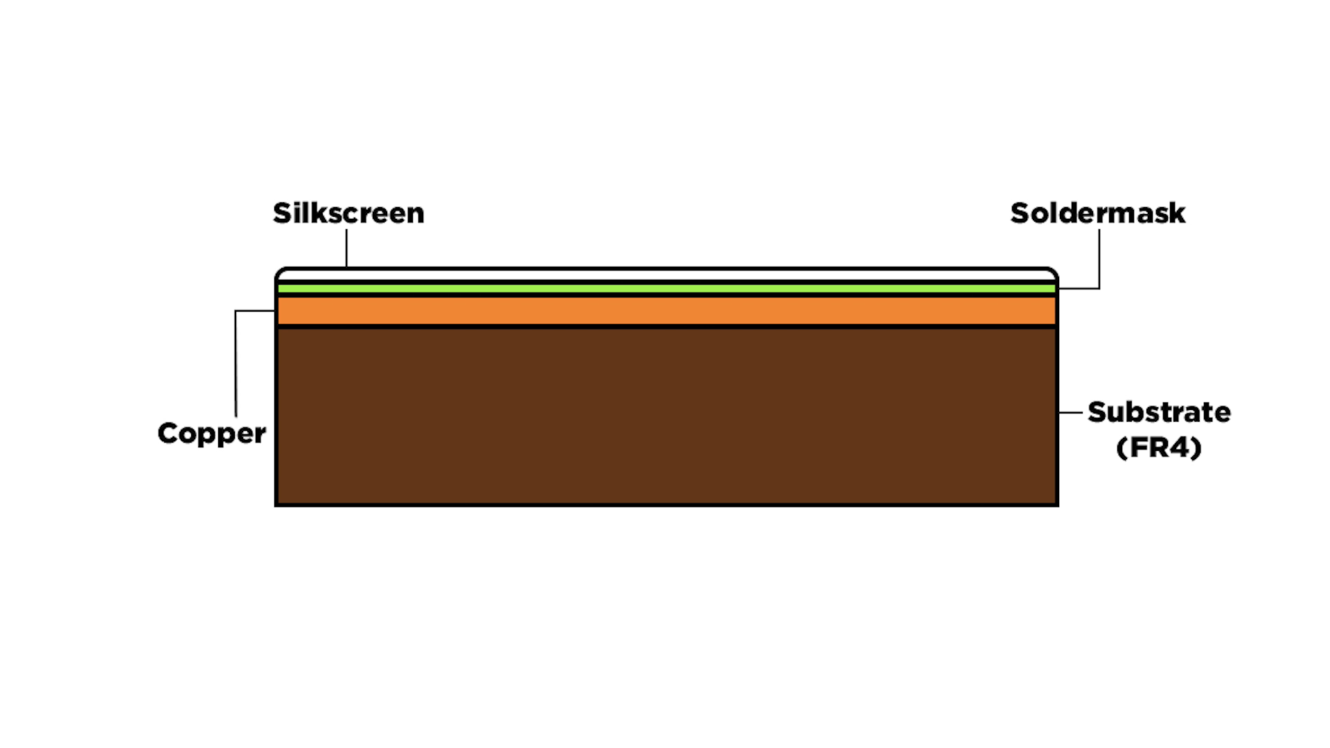
First, we have the substrate. It’s a fiberglass (FR4) material, which is the solid core that gives the PCB its rigidity and thickness. It mechanically holds the connections and the components, just like this Perfboard (zero PCB) or like a breadboard.

Conducting Layer
Then we have the layer conducting layer. In most cases, this conducting layer is made of copper and connects the electrical connection between the components just like traditional wires.

Traces
These connections are called traces, and they can be of various widths and lengths depending on what we are planning to connect, which we’ll discuss in more detail as we make our own design.

Multi-Layer
When we say ‘Layers‘ in a PCB, like a single layer, a double layer or a multilayer, it generally refers to the number of conduction layers in the PCB.

We can actually stop production at this stage by just having the base layer and the conduction layer because we have a usable PCB that does its function.
Are All Layers Required?

For example, look at the PCB shown in the figure above; it’s a little different than what we come across in day-to-day life. They come in this green layer on top.
This is called the Solder Mask (as shown in the figure below). The solder mask protects the PCB surface and insulates the copper circuit from oxidation. It also prevents accidental contact with other metal, solder or conductive bits. It can be of any color, but mostly it’s green because it’s easy on the eye and also because it’s easy to differentiate between traces, planes and empty spaces.
Solder Mask

However, the solder mask doesn’t cover up everything on the board. It’s applied in such a way that it covers up the small traces and empty spaces but exposes some space around the component pads so they can be soldered later.
Silk Layer
Finally, we have the Silk Layer. This is the topmost layer with names, letters and symbols, and it is usually white in colour. It makes the assembly and final working of the PCB way more convenient, and it does not add any physical or electrical features to the PCB; it’s mostly just for appearance.

KiCad PCB Stackup
Coming back to the topic on KiCad, the PCB layout editor is pretty simple to use, and it uses the same buttons and navigation style as the schematic editor.

To open the PCB layout editor, either select that option directly from the project page or go to the schematic window and click on the ‘Open PCB in board editor’ option from the top toolbar.
It’ll open up an empty PCB layout editor, which is pretty simple to use. You can use similar buttons and navigation styles in the schematic editor that we have learned. Since we know the basics, we can directly start with the PCB stack-up that we discussed in this article. So, let’s start with setting up the board. Click on the board setup icon.

Under that, select the ‘board stack up’. As shown, KiCAD automatically selects board editor layers.

Here, the prefix ‘F’ stands for ‘front’, and the prefix ‘B’ stands for ‘back’. It is referring to the front and back sides of the PCB. Based on the prefixes, we have several layers that are used in a PCB. Let’s cut down on layers that are not necessary for our project. But before that, let’s go through a few things that we haven’t discussed yet. First, we have ‘F. Courtyard‘ and ‘B. Courtyard‘. This layer defines a safe area around a component, so while assembling the physical components, they don’t overlap each other.

Then we have the F.Fab and B.Fab. Using these two layers, we can give more data to manufacturing without including them in our final design, like mentioning some important points or notes. For now, let’s turn it off (uncheck), as we won’t be using both of these layers for this tutorial.
Then we have the ‘F.Adhesive‘ and ‘B.Adhesive‘ layers; this layer would be required only if the component is not easy to mount and requires additional glue. This layer would indicate where the glue or adhesive should be applied and where it shouldn’t. Let’s turn this off (uncheck) as well, as our circuit doesn’t need it.
Then we have ‘F.Paste‘ and ‘B.Paste‘, they have information about where we shouldn’t apply the solder mask so we can solder the components. Also, these layers are essential in making stencils, which we’ll discuss in a future article. Sometimes, these layers are also referred to as ‘Stencil Layers‘.
By now, one should be familiar with the following layers: F.Silkscreen layer, F.Mask layer, F.Cu layer (which stands for conduction layer or copper layer), and similarly, we have B.Cu, B.Mask, B.Silkscreen for the back of the board.
Finally, we have ‘Edge.Cuts‘. This layer defines the PCB shape and dimension. The next one, ‘Margin‘, is used for defining the areas where the components, traces and any other part of the PCB are allowed to be placed or not placed.
The ‘User.Eco‘ layers are used only if one is sharing the PCB layout file with other engineers, where we can include the revision number of the PCBs or any other graphics or drawings that won’t be in the final product. Since that is not our current case, we can uncheck that as well.
We can also turn off the drawing and comments, which are generally used for user reference and have little to do with the PCB. Finally, we can also turn off ‘User layers‘, which are user-defined layers where we can add special features to the PCB and also convey them to the fabrication plant. Now, just click the okay button after unchecking all the not required layers.
Next, we have the ‘Physical Stackup‘; this is where we assign the number of layers. In our case, we’ll be using just one layer to make our PCB. As a beginner, one need not mess with the rest of the settings; most of these values will be taken care of by the fabrication plant.

Board Finish
Then we have the ‘Board Finish’, which gives us various options to have a surface finish for our PCB. We have a dedicated article just discussing board finish, so please check it out!

Solder Mask / Paste
Then we have ‘Solder mask/paste’. We can use the information provided by the manufacturer website and fill this information but in most cases, you would get pretty good results with default values. So we’ll leave it to default for now.

Text & Graphics
Next We have the ‘Text & Graphics’, these settings are just for appearances and it doesn’t affect the PCB in any way. We can change the line thickness, text and other information.

This brings us to the end of this article. In the next article, we’ll add some design rules and bring all the footprint to start with PCB layout. if you have questions you can always reach out to us at PCB CUPID here. Until then keep learning and keep creating!


Leave a comment