
In the previous article, we made an average looking circuit using the schematic editor by using the bare minimum tools that KiCAD has to offer. In this article, we’ll discuss more interesting tools and make the same schematic more presentable.
Page Settings
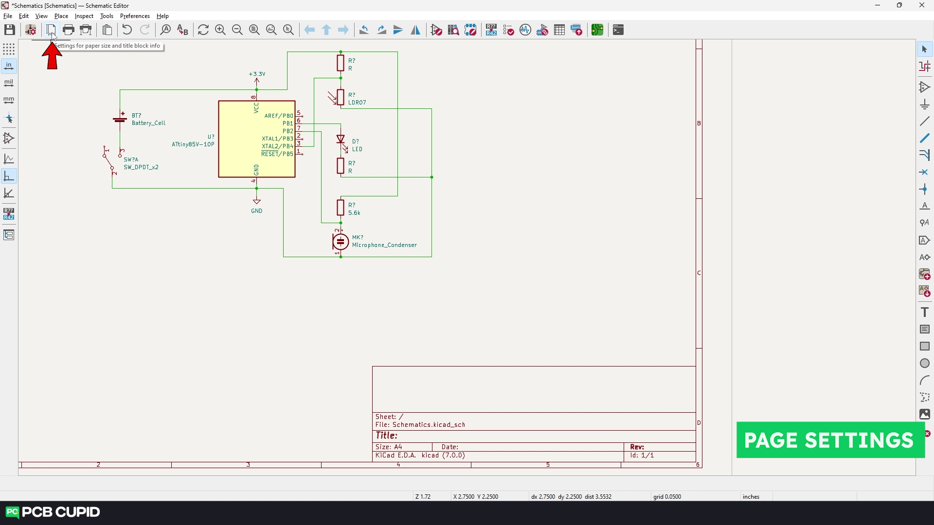
Let’s start by adding essential information to the document, like adding author name and other information that we like to add about the circuit (like a date or description). To do that, click on page setting icon and add the information that’s required.
Let start by adding date, we can either use the current date or we can also add a custom date. Then followed by we’ll add the number of revisions that we are working on, for now the circuit is currently version 1 so, V1.

Then we’ll add the title of the project followed by the company. Use comment option to add more information to the document. A custom template can also be added. Let’s keep that topic for another article.
Once the data is filled just hit okay. As confirmation, you can see the entered details on the right bottom part of the document.

Net Name
Now, back to the circuit. Just like the components, each connection has its own name, that’s called ‘Net name‘. When we click on the connection and look at the bottom status bar we can see the name of the connection.

This is one of the powerful features of KiCAD. Even if the connection is not manually made, but the two components have the same net name then, they we’ll be connected in the backend by KiCAD. This is great because we can avoid overlapping and having way too many connections going across the drawing sheet.

The names GND and 3.3V are automatically assigned by the power symbols. But this is not the case for all connections. When we click on other connection (say the one connecting to the resistors), we can see that net does not have any name (<NO NET>). In that case we can create a custom net name for the connection.

In the toolbar select the tool called “Add net label” and click on the net that we need to add the name.

While adding net label, one is free to choose whatever name they want but we would suggest keeping them meaning full, not to use some random letters or symbols. Follow the same process for the rest of the connection, which should result in the below figure :

No Connection Flag
Now, there might be situations where few pins are not being used, like pins 1, 3 and 5 of ATTINTY in our case. This can be little troublesome later down the road, also while performing Electrical Rules Check (ERC), it doesn’t clearly communicate what those pins do. So KiCAD provides a ‘No connection‘ flag that we can use, which make sure we don’t accidently connect any components to it.


Automatic Annotation of Schematic
Now, let’s fix the values and designators. We have discussed about editing values in the previous articles, refresh your memory here.
To fix designators, go to the “annotation tool” on the top bar.

Make sure the entire schematic is selected (and select the ‘reset existing annotation’) and click on annotate.

This will automatically add numbers to the components.

Text
Since there are no more annoying crossover connections we can create sections of the circuit which are easier to understand. We can name the sections using the text tool. The option of changing the appearance is also there but we’ll stick to default for now.

Tip: just copy the text using ‘Ctrl + C‘ and paste where needed using ‘Ctrl + V‘ and to edit the text, use the shortcut ‘E‘
After naming the section the circuit should look like this:

Graphics
To clearly define the sections we can use graphics tools (bottom set of tool on right tool bar).

Just select the tools and mark the area, and to change the appearance select the graphics and press ‘E‘.

Once done, the circuit should be something like this:

This clearly makes the whole circuit readable, easy to understand and gives a clean look, doesn’t it?
Images & Logo
To make it much better we can also add logos and images to the circuit if you wish. You can do that by using the ‘bitmap image tool‘.

TextBox
By using a textbox, it’s easier to share this circuit online and or have a link to a website or a project page.

The text box feature is new for KiCAD 7.0, previous versions of KiCAD (5.0 and 6.0) did not have it.
Conclusion
This completes the features of Schematic editor. If you like to watch this as video tutorial please check this out :
In the next article, let’s look at one crucial step that we’ve to perform before moving to PCB layout editor. Until then if you have any questions or doubts leave them here.
Keep learning and keep creating!


Leave a comment