In the last aritcle, we discussed various factors on how to select the right footprint for your components. Now, we’ll discuss how we can assign the footprint to the components using the KiCad’s footprint assignment tool. Footprint Assignment Tool Here ...
PCB CUPID Latest Articles
How To Select The Best Footprint?
In the previous article we completed the schematic with ERC and prepared it for PCB development. But each symbol in the schematic is just a representation of the component and it does not contain the information about the physical properties ...
How To Perform ERC & Verify Circuit In KiCAD
We have finally completed making a circuit using the schematic editor! We are very close to making our own printed circuit board. All we have to do is some Electrical Rule Check (ERC) and footprint assignments to start with the ...
What is PCB Stackup & How to Setup in KiCad

We finally finished assigning the components in the previous article. In this article, we’ll discuss a little about the PCB layers and how to co-relate the physical PCB to the PCB layout editor. PCB STACKUP Printed circuit boards are made ...
How To Prettify Your Schematic with Kicad 7.0

In the previous article, we made an average looking circuit using the schematic editor by using the bare minimum tools that KiCAD has to offer. In this article, we’ll discuss more interesting tools and make the same schematic more presentable. ...
How To Design a Circuit in KiCAD’s Schematic Editor
KiCAD is such an incredible software which is completely free! But those who are just getting started might get overwhelmed by the amount of options and settings it has to offer. So learning each tool without real world examples would ...
How To Use New Kicad User Interface
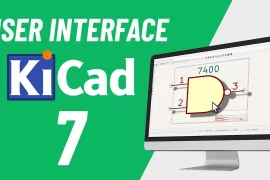
In the previous article we talk about what is KiCad and some of the tools it has to offer. In this article, we’ll try to explore more about KiCad, specially how to navigate around KiCad and how some of its tools ...
GitHub For Hardware Engineer But Better: CADLAB.IO

Working on the PCB designing software can be tedious if you want repetitive updates, modifications, while simultaneously sharing the project with your teammates or your manufacturer. Is there a way to version control your PCB designs and collaborate with teammates ...
New Launches in Adafruit Feather Series!

Adafruit has launched a trio of new boards, out of the three, two aim at those working on automotive or other CAN bus projects and one which gives you an easy way to hook a Raspberry Pi RP2040 microcontroller up ...
LinkMicro LM246MS Microscope For Soldering And Easy Repair

As an electronic enthusiast, hobbyist or a professional you understand the importance of magnification needed while assembling or examining electronics, especially working with SMD components. Therefore, a good magnifying device or an electronic microscope is needed. There are many microscopes ...


