We have finally completed making a circuit using the schematic editor! We are very close to making our own printed circuit board. All we have to do is some Electrical Rule Check (ERC) and footprint assignments to start with the PCB Development.
Electrical Rules
It’s always good to double check, because there is usually a high possibility that we might make some mistake. So KiCAD offers some basic checklist that would help us build a very robust circuit with minimal error. You can see this checklist on the schematic setup under ‘Electrical Rules‘.
Go to the toolbar and click on the ‘Schematic Setup‘

Click on the Electrical Rules on the pop up window as shown in the figure.

Here we can see all the rules that KiCAD has previously set up. For example, pin not selected, symbol is not annotated, etc. This takes care of a lot of tiny details that we easily miss out on (We strongly suggest not changing any default settings unless you know what you are doing).
Electrical Rules Checker (ERC)
Now let’s see how to perform ERC and see if our circuit passes all those rules.
On the top toolbar we have the option ‘Perform electrical rules check‘, click on it and then click on the Run ERC.

You can see, we’ve one warning and three errors.

Fix ERC Errors
Let’s fix the error first then move on to warnings. For now, we’ll uncheck the warning in the pop up window and start with the first error ‘pin not connected‘ . Just click on the error and it will take us where the error marker is located.
Here, we can see that I have forgotten to add a ‘no connection flag‘. When we add a no connection flag, it let’s KiCAD know that we are willingly giving up the pin and it’s not an accident that we have missed connection to those pins. So, make sure to add no connection flag to all the unused pins in the circuit.
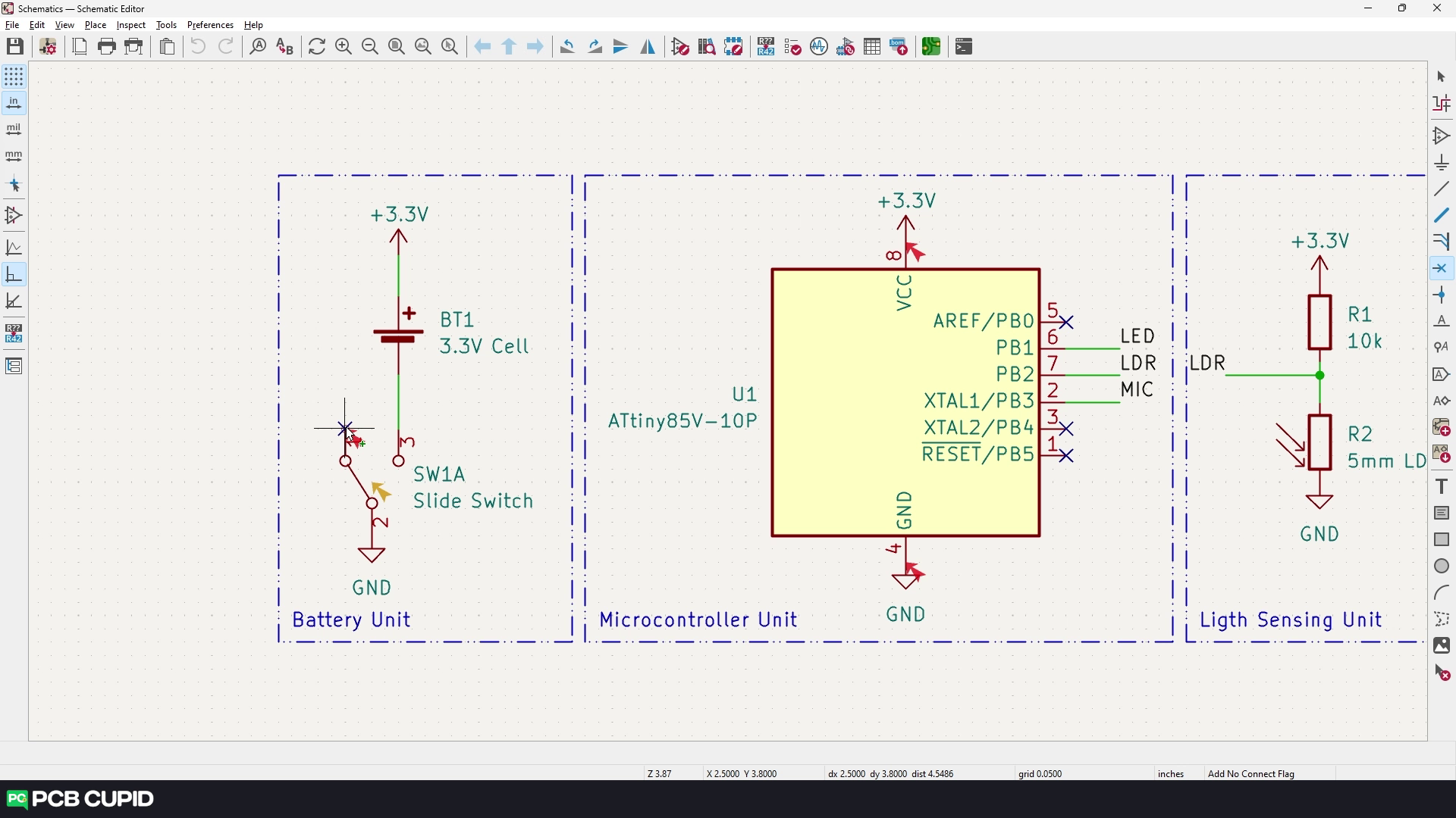
Once the error is fixed run the ERC again. You can see we have resolved the error message and making a very good progress! We just have one warning and two errors to go.

These two error mean that KiCAD doesn’t know which net carries the power and how the components are powered. To fix this, go to ‘add power symbol‘ (on the right tool bar) and search for ‘Power flag‘ and click on ‘PWR_FLAG‘ and add the flag to to VCC and GND net.

We can run ERC again, and all the error and messages should be resolved.

Fix ERC Warnings
Now let’s move on to warnings and fix that.
When we select the warnings check box, the warning says that the switch SW1 has one unplaced unit.

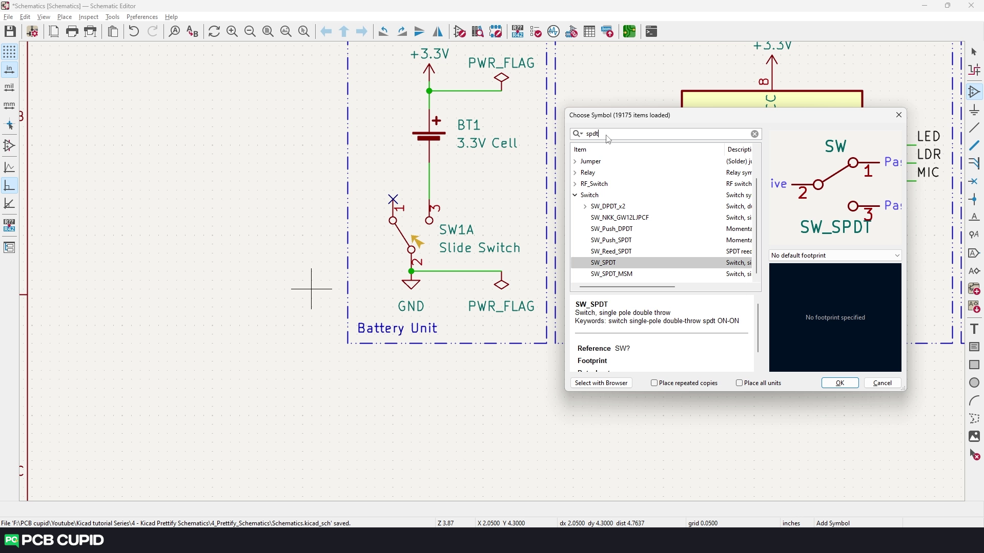
To understand this warning better, let’s take a look at the symbol we’ve placed. When we try to add the same switch, we see it contains two units. ‘Unit A‘ and ‘Unit B‘.

This is because KiCAD is trying to simplify the Double Pole Double Throw switch into two Single Pole Double Throw switches. It is still technically correct and the circuit we have built is still good. We can also go ahead with the circuit while ignoring the warning because this is just a symbol that represents the switch and doesn’t have to do anything with the physical dimension or the shape of the switch.
But let’s try fixing the warning. To do so, search for a single pole double throw switch and replace it with the existing switch.
Now let’s try ERC. Now the ERC have zero errors and warnings. Perfect!

This errors and warnings are just for reference but in reality you can face a lot more errors and warnings. Unfortunately, covering each one of them wouldn’t be possible in this article. But lucky, most of the errors are readable and self explanatory. In any case if you need any help, you can always reach out at PCB CUPID Q&A.
So far we have completed the schematics and this is perfect to share and showcase the circuit. But most of the components here on the circuit are generic; meaning, we just use the resistor and its value, unaware of the type of resistor (through hole or surface mount), also we are not sure what is the wattage of the resistor or, a few components might have different brands which might have same functionality but totally different physical dimension and appearance.
To fix this, we have to assign ‘footprint‘ to these symbols, which we’ll be learning in the upcoming article. Until then Keep learning, keep creating!


Leave a comment