
Lithium batteries have become very popular in recent years, mostly due to EVs popping up everywhere. These batteries are perfect for storing higher energy levels with a very small footprint, but where there’s immense power, there’s an element of risk lurking! ...
PCB CUPID Latest Articles
1: How To Design PCB in EasyEDA : Introduction

EasyEDA simplifies PCB design with cloud-based accessibility, collaborative tools, and a user-friendly interface. Usually, professional CAD software needs beefy computers, or at least decent hardware, to run most of its features. But in recent years, cloud-based tools have become very ...
JLCPCB: Selling PCB At Bargain, Starting from $2

With the rising demand of PCBs in electronic devices and advanced technology there is a rise in PCB manufacturers all over the world. Today one such PCB manufacturer with world over presence will be unwrapped and analysed in detail is ...
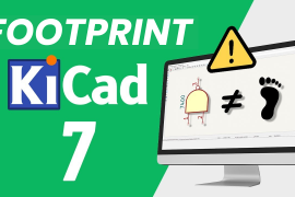
How To Use KiCAD’s Footprint Assignment Tool
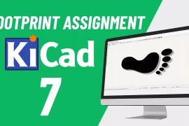
In the last aritcle, we discussed various factors on how to select the right footprint for your components. Now, we’ll discuss how we can assign the footprint to the components using the KiCad’s footprint assignment tool. Footprint Assignment Tool Here ...
How To Select The Best Footprint?
In the previous article we completed the schematic with ERC and prepared it for PCB development. But each symbol in the schematic is just a representation of the component and it does not contain the information about the physical properties ...