In the previous article we completed the schematic with ERC and prepared it for PCB development. But each symbol in the schematic is just a representation of the component and it does not contain the information about the physical properties of the components (like number of pins, shape and size). That’s the reason we need to assign the symbol to a physical counterpart called footprint.
What is Footprint?
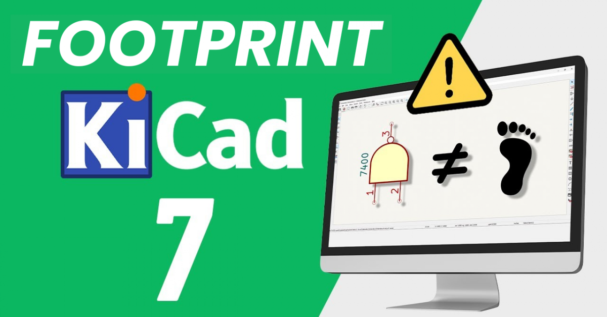
Do you get the idea why it’s called footprint? It’s because we consider the 2d cross section of the component and how it’s placed. For analogy we can consider a human footprint.

Just by seeing the footprint we can figure out how the person was standing and in some cases what he was trying to do. Similarly we can use component footprint to determine the orientation and the placement of the component.

Since we nailed down the basics, let’s see how we can assign footprints in KiCAD.
Assignment Tool
Open the footprint editor from the top bar.

You can see some of the components are assigned by KiCAD and some unsigned components are highlighted in yellow (shown in the figure below).

It’s not possible to have the footprints for all the components in the world, but KiCAD does have a huge collection of footprints. In case if you are not able to find the required footprint, in later article we’ll discuss how we can make our custom symbols/footprint as we’ll as use 3rd party symbols/footprints.
Let’s quickly take a tour of this footprint assignment window. At the left, we have all the component names, example: resistor, capacitor, diode and LED. And on the right we have the actual footprint for each of the components. To view them, just do a right click and click on ‘view selected footprint‘. This will take us to a window which shows us the 2D cross-section of the component.

Most of the tools and navigation are similar to what we had in the schematic editor. To view in 3D, press ‘Alt + 3‘ or click on the ‘Show 3D viewer‘ icon from the top bar.

Once you confirm the component footprint we can assign them to the symbols.
How To Select Correct Footprint?
Before assigning a footprint we need to consider a few key points:
- Can we source the component? Just because the footprint is available on KiCAD doesn’t mean we can get the actual component easily. Make sure to search for the parts and see if it’s easier to source. More importantly check if it’ll be available after a few months or even after a few years? If the design and the components aren’t chosen properly, the PCB we’ll be obsolete very soon and might have to be redesigned.
- Is the component cost effective? Always check if the components are cost effective. The whole reason to build a PCB is to keep the cost down during production while doing higher quantities. So even a small difference for one PCB can make a huge difference while mass manufacturing.
- Does the component match the datasheet? Each component will have a datasheet along with its footprint and its physical dimension. Just double check if your footprint is matching the datasheet dimension.
- If possible get the components hands on. Don’t do guess work or don’t just rely on a datasheet if the vendor is not trust worthy. Some vendors may provide a totally different datasheet and supply completely a different part, it takes time and experience to find a reliable vendor who can ship the promised product at low cost and fast.
- Can machines assemble it? We can sometimes choose the low cost component or a part that works for the circuit which has to be assembled manually, it should be fine if you are doing only a few PCB or planning to manufacture a smaller quantity. But this would increase the cost very high during large production because manual labor is way more expensive than machines.
These are just a few points and there’s a lot more to consider as you skill up!
You can watch this complete article as a video here :
In the next article, we’ll continue working on the same project further and finish assigning the footprints. And later we’ll see how to take the entire circuit inside the PCB editor and start building PCB!
Until then, if you have any questions or doubts you can reach out to us using PCB CUPID Q&A.


Leave a comment