In the previous article we talk about what is KiCad and some of the tools it has to offer. In this article, we’ll try to explore more about KiCad, specially how to navigate around KiCad and how some of its tools work.
To follow along this tutorial, download the example project from our Github Repo.
Open the downloaded project in KiCad and then open the schematic file.
Don’t get overwhelmed with the amount of icons and tools on the schematic editor, let’s take baby steps and focus on a few tools at a time.
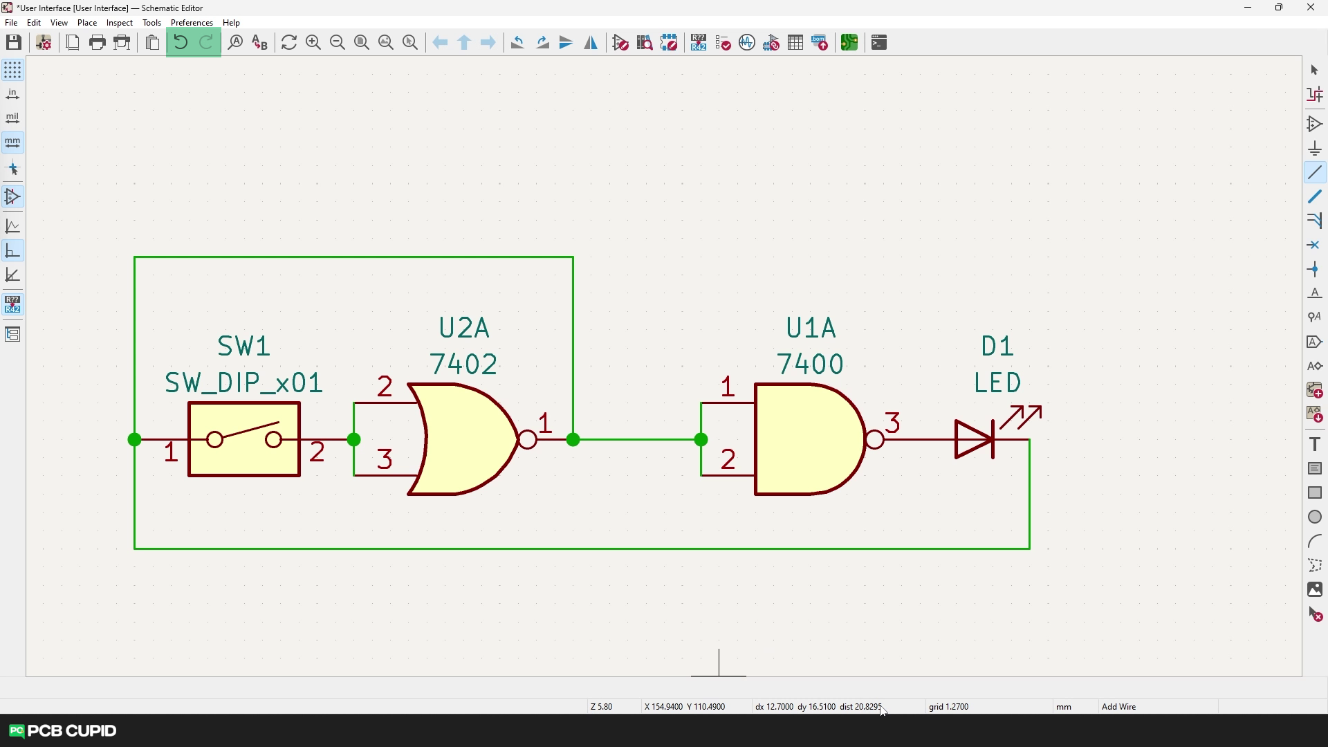
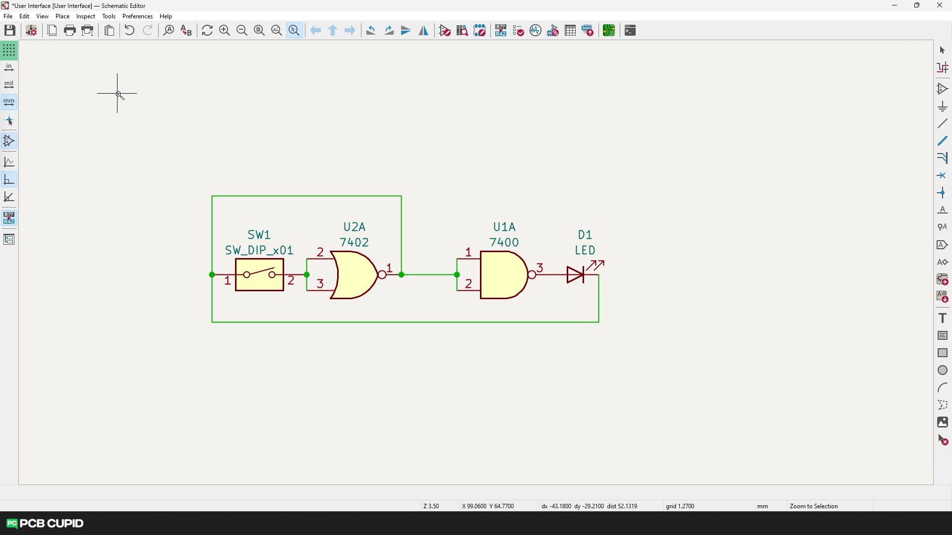
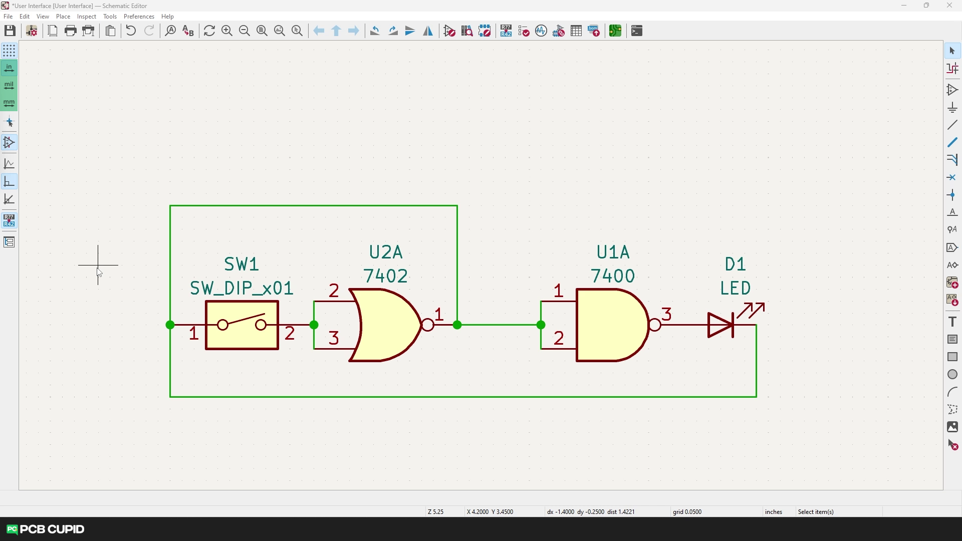
The Image below shows the schematics and how the connections are drawn between the components. To zooming in and out, you can use the scroll wheel on your mouse and to move across the document, either use the middle (Scroll) click drag or use right click drag to pan.
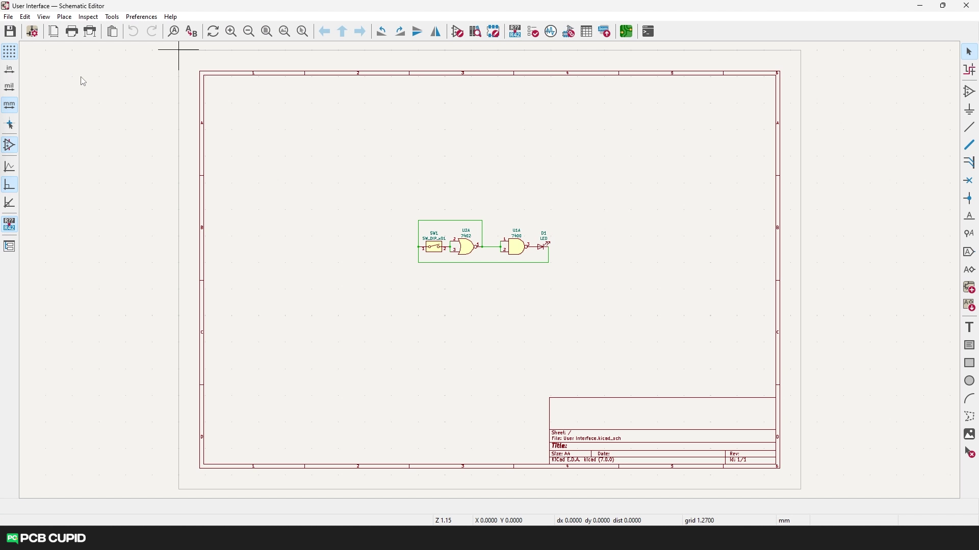
When we look at the status bar closely, we have information about the zoom level, X and Y co-ordinate of the cursor and the distance the cursor travels. For example, when we want to know the distance between the two components (shown in image), place the cursor on the first component and press space bar to reset the ‘dx’ and ‘dy’ value on the status bar. Then move the cursor to the second component to see the distance. This feature will come very handy when working with a PCB editor rather than the schematic editor. Please check out the video for better understanding on how it works.
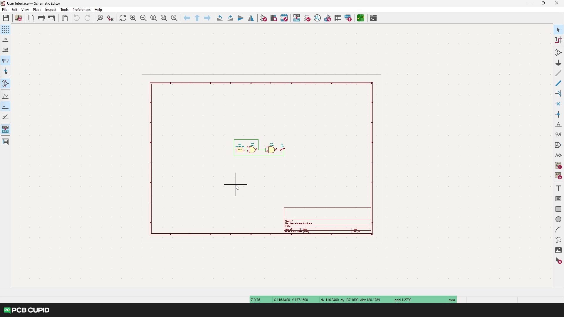
If you zoom in enough, you can see small points where the cursor snaps on too. These are called the grid points which we’ll be of great help when connecting two components together so we don’t have to fiddle around to connect them properly and the distance between them can be seen on the status bar as well.
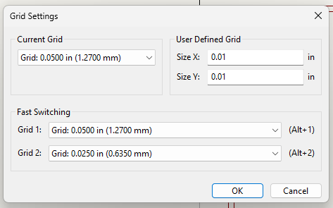
But try not to mess around with the Grid settings on schematic editor , try to keep the grid settings to 1.27mm or 50mil. You can do that by following the below steps:
- Go to View on the menu bar
- Click on Grid Properties
- Set current Grid to 1.27mm or 50mils
Toolbar
There are more helpful navigation tools on the top toolbar.
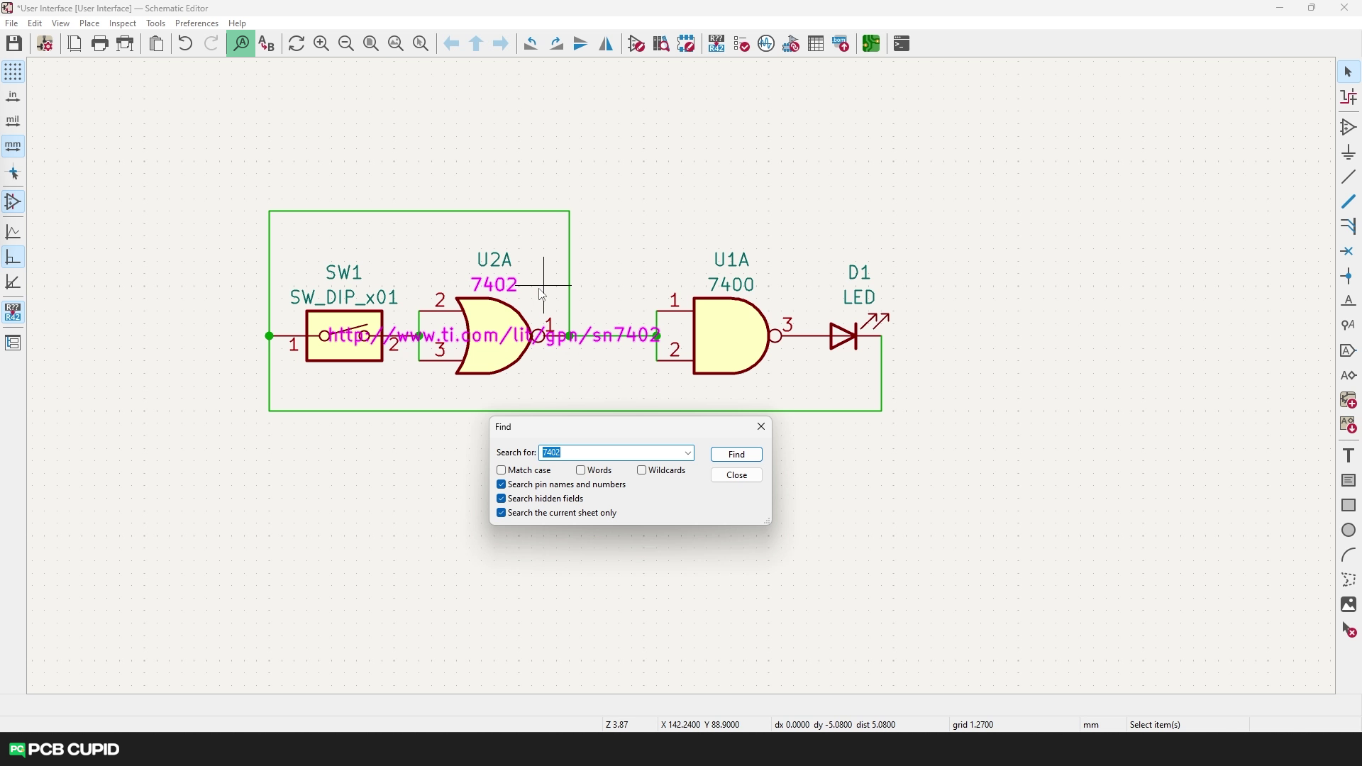
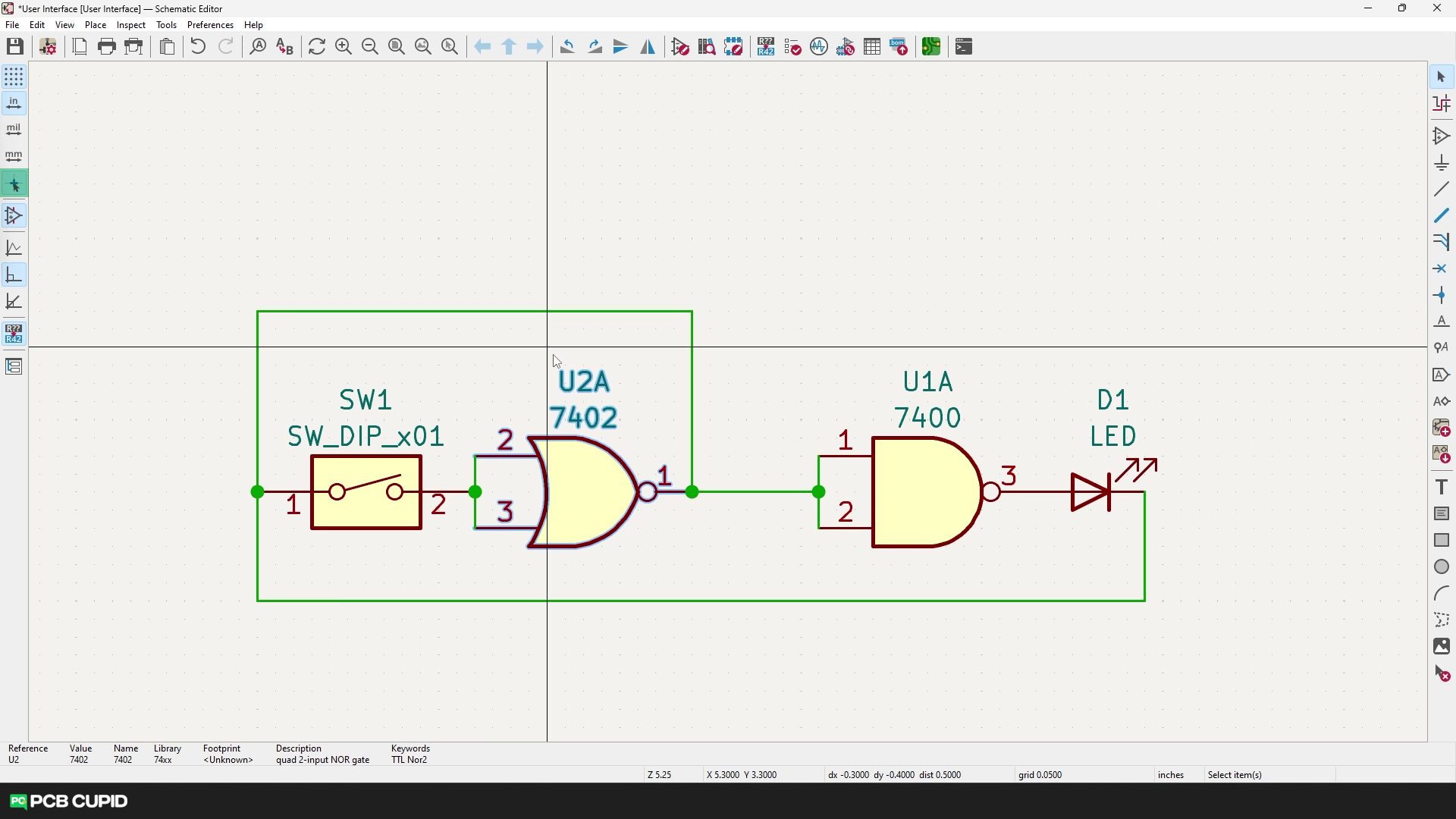
These two buttons can be used to ‘undo’ (Shortcut : Ctrl + Z) and ‘redo’ (Shortcut : Ctrl + Y) any changes made, followed by that is ‘find’ (Shortcut : Ctrl + F) to search items on the schematic. Once the item is found, it is highlight in pink.
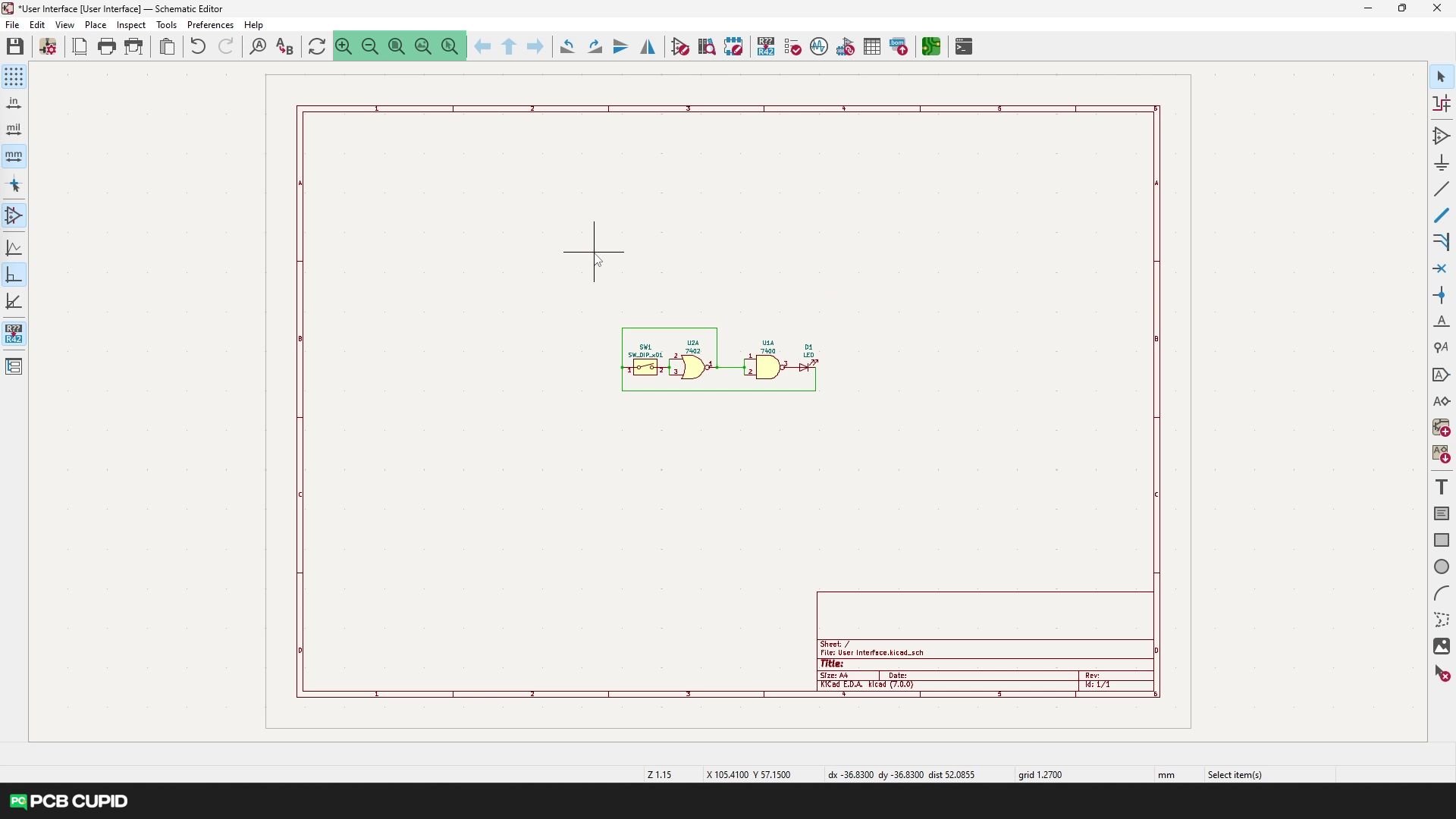
When you are unable to zoom in and out using scroll wheel or your working on a Laptop (please don’t use laptop), these buttons on toolbar can come in handy. The ‘+’ symbol zooms in and ‘-‘ symbol zooms out. Next is ‘Zoom to fit’ , will fit the entire document to the display. Next, the ‘Zoom to objects’ will fit just your schematic to the screen. Finally, ‘Zoom to selection’ will zoom and fit to display the particular area that is selected by you.
Tools on the left bar
Grid:
The dot matrix-like icon is for turning on/off the grid. It’s useful when you like to take a screenshot or maybe want to have a better look at the schematics.
Units:
The next three buttons will help in setting the document units. It can be inches, mils or mm. In all our project all dimensions and calculations will be based on mm.
Full Crosshair:
The ‘+’ graphics that follows the mouse cursor is the crosshair, and you can toggle between full screen and short crosshair using this button. In most cases the short crosshair is preferred but when two components needs to be aligned, switch to full crosshair, that is more helpful.
Hidden pins:
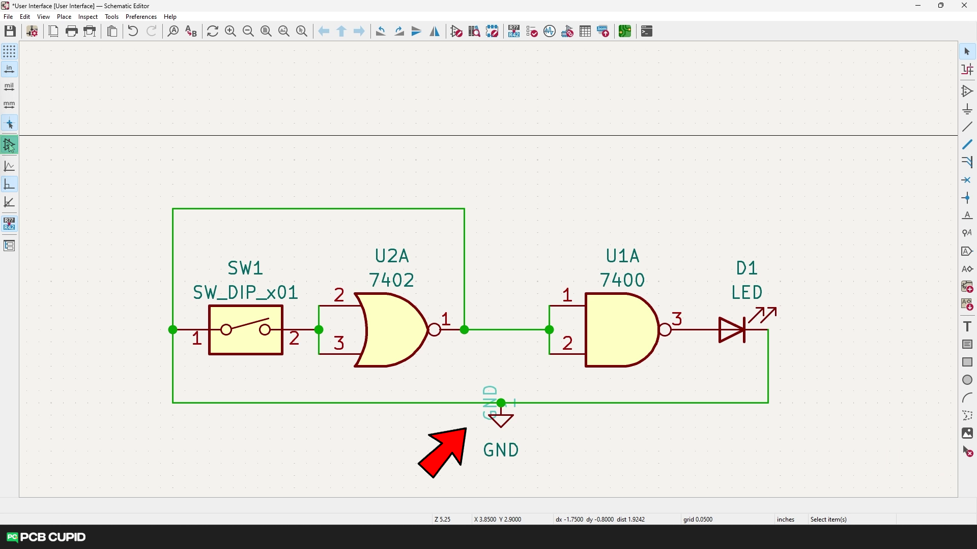
his button will hide/unhide the hidden pins which are usually created along with the power symbols.
Turn on and off the bus angle:
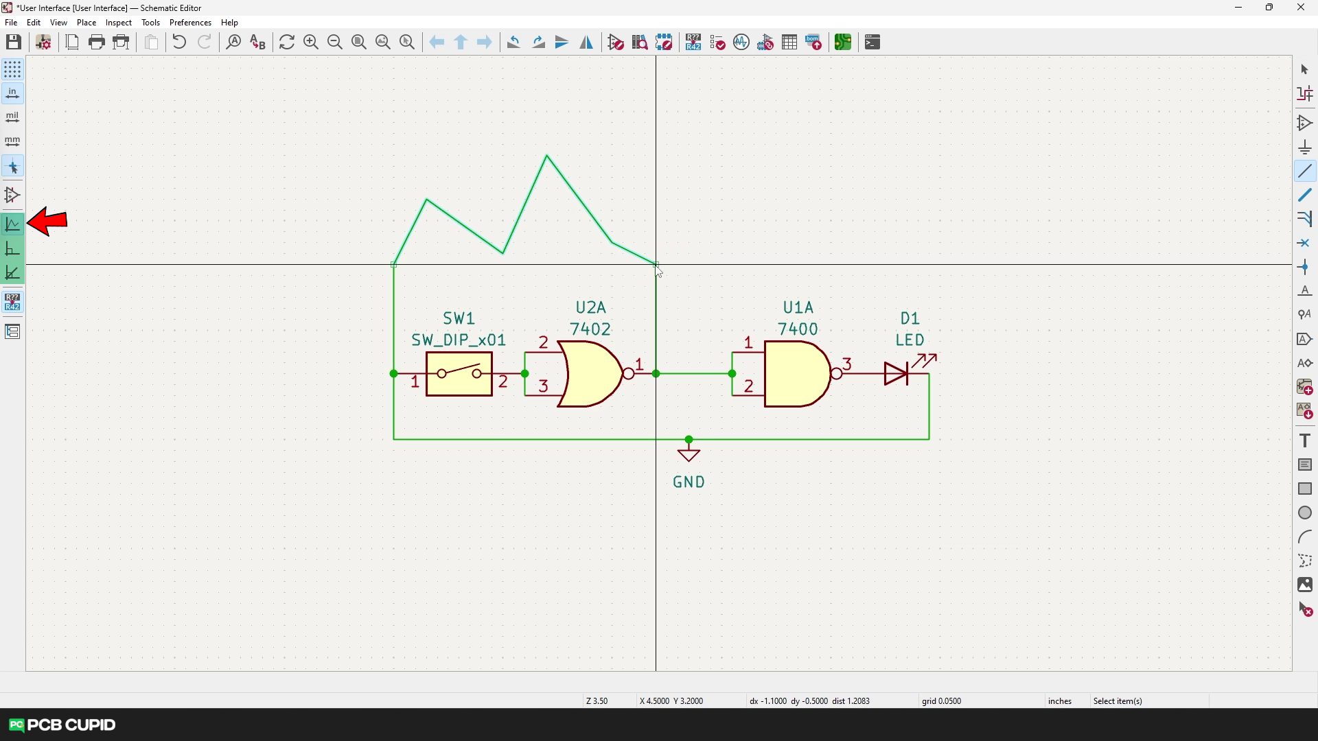
The next three buttons will help in the angle of the wire that’s connecting between two components. The first button lets the wire angle to be any degree. When you make a click, the wire takes that shape as shown in the figure.
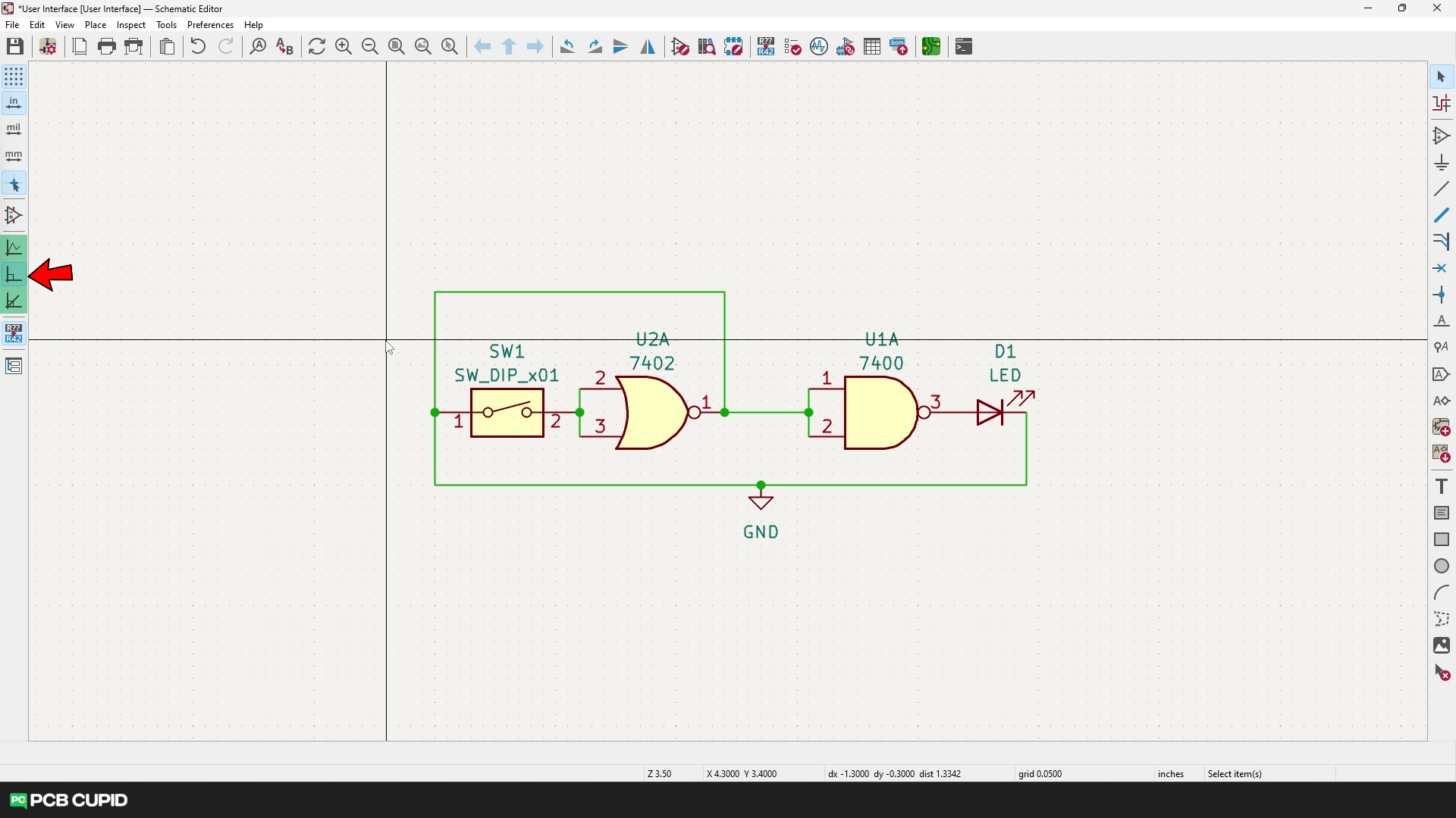
The next button contraints the wire angle at 90 degrees as shown in the figure below.
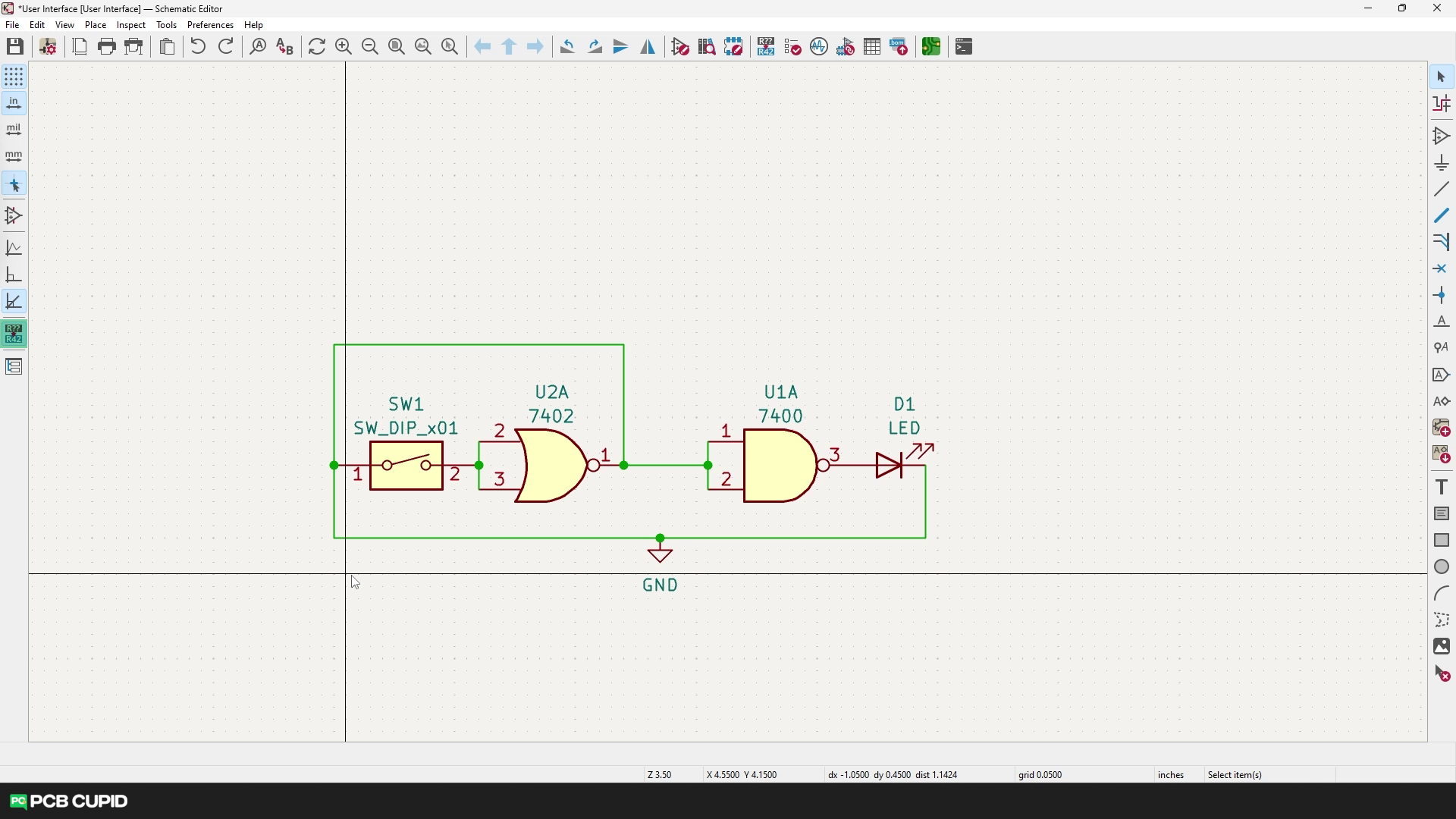
The last angle option lets you switch to 45 degrees as shown in the figure below.

Automatic annotation:
The name (ID for each symbol) auto generated by KiCad like SW1, U2A etc. are called designators. You can keep this automatic annotation turned on to create the number for each new component automatically as you place or you can turn it off and name all the components at the end (Using Annotation tool).
We prefer the latter method, where we turn off the automatic annotation. Which will help us in keeping the number consistent just in case if we delete some symbol in between while drawing the schematic.
The last button, ‘hierarchy navigator’ will be discussed in future articles as it is a tad bit complicated for beginners.
You can watch this tutorial as a video here :
In the next article, we’ll see how we can use other tools that are on the right side along with creating our first schematic.
If you have any questions regarding the topics that we are discussing or any other questions related to PCB, you can always reach out to us at PCB Cupid forum. More articles to follow. Feel free to share these articles with people who might be interested and until next time, keep learning and keep creating!


Leave a comment