
Making PCBs more reliable and durable is done through selection of substrate, laminate and board type. Further, surface finishing is done by coating certain material on the board. A PCB surface finish is an intermetallic joint between the bare copper of the solderable area of the printed circuit board and the components.

PCB Surface Finish
Necessity of Surface Finish:
PCB surface finish plating is needed because it:
- Prevents the copper of the substrate from oxidation and hence corrosion.
- Increases the solderable surface of the components on the board.
- Strengthening solder connections.
- Increases protection of copper traces.
Types of PCB Surface Finish:
Depending on the type of coating used for surface finish and other specifications, there are many types of PCB surface finishes available to choose from:
- ENIG: Electroless Nickel Immersion Gold
- HASL: Hot Air Solder Level
- Lead-Free HASL
- Immersion Silver (Au)
- Immersion Tin (Sn)
- ENEPIG: Electroless Nickel Electroless Palladium Immersion Gold
- Electrolytic Wire Bondable Gold
- Electrolytic Hard Gold
Some of the above mentioned types will be discussed in detail along with their pros and cons.
The last three mentioned are high-end surface finishing which are used for high-end products due to the extra cost involved.
There are organic surface finishing options available too; they use organic compounds to form a protective coating over the copper layer on the PCB. The following types are:
- OSP: Organic Solderability Preservative
- Carbon Ink
These are used for RF shielding and keypads, etc.
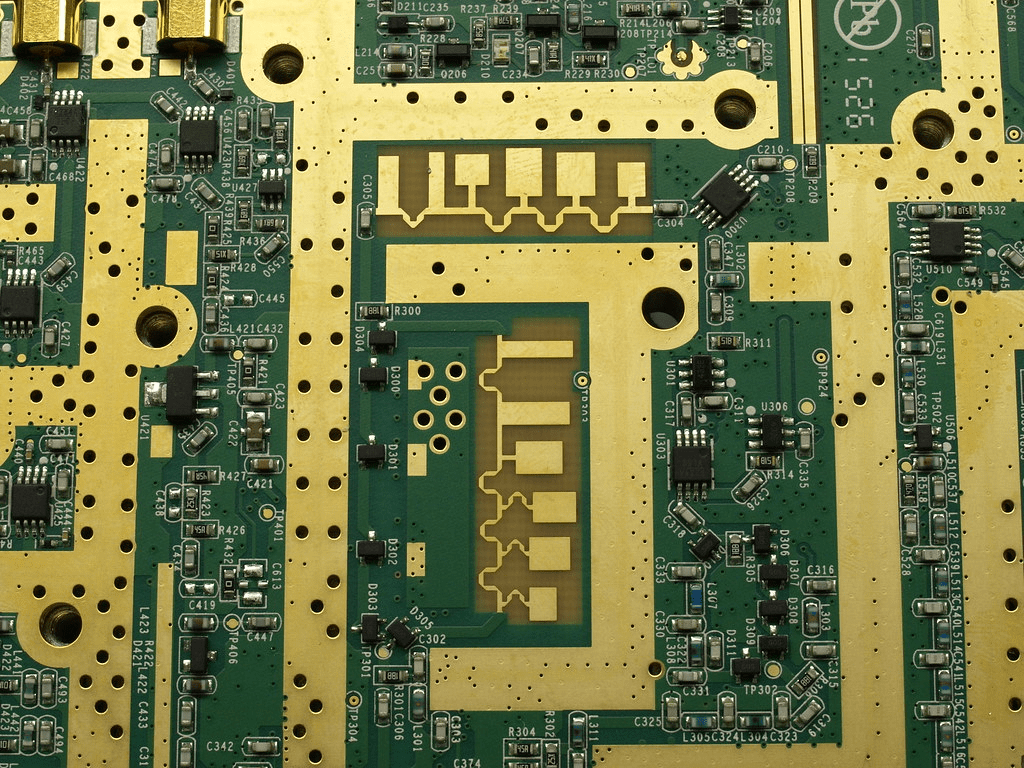
ENIG: Electroless Nickel Immersion Gold
In ENIG, electroless nickel plating is covered first followed by a thin coating of immersion gold, shielding the copper from oxidation.
ENIG plated PCB
Chemical Reactions for Nickel-Plating:
Primary Reaction: Ni2++H2 PO2-+H2O→Ni+H2PO3-+2H+
Secondary Reaction 1:
H2O+H2 PO2-H2+H2PO3-
Secondary Reaction 2: 2H2 PO2-→P+H2PO3-+OH-+12H2
Chemical Reaction for Immersion Gold:
Anodic Reaction: Ni→Ni2++2e-
Cathodic Reaction: Au(CN)2-+e-→Au+2CN-
Overall Reaction: Ni+2 Au(CN)2-Ni2++2Au+4CN-
Advantages:
- Provide contact conduction, bonding and other functions to meet a variety of assembly requirements.
- It is RoHS (Restriction of Hazardous Substances) compliant.
- Excellent surface flatness and it is suitable for small spacing components such as BGA components.
- Interference to the signal is relatively small since only nickel and gold is coated over copper.
- Excellent solderability and better stability.
- Easy and fast process.
Disadvantages:
- Relatively expensive compared to other surface finishing types.
- Occasionally cause black pads or nickel corrosion on the surface.
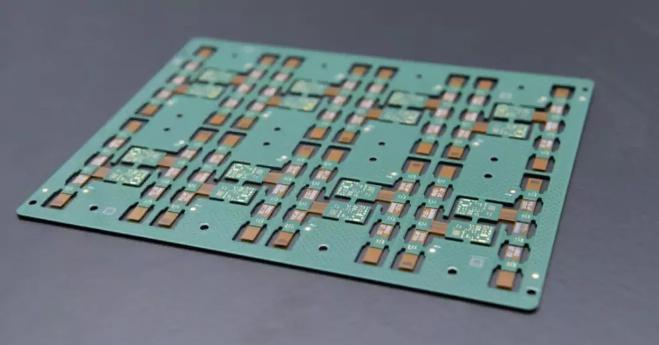
HASL: Hot Air Solder Level
For coating the pad with tin-lead solder a hot air solder levelling method is applied.
Preparing the PCB
Before coating, the panel is passed through the preparation line where they are cleaned of impurities. The copper is etched to remove oxides and flux is applied to the surface.
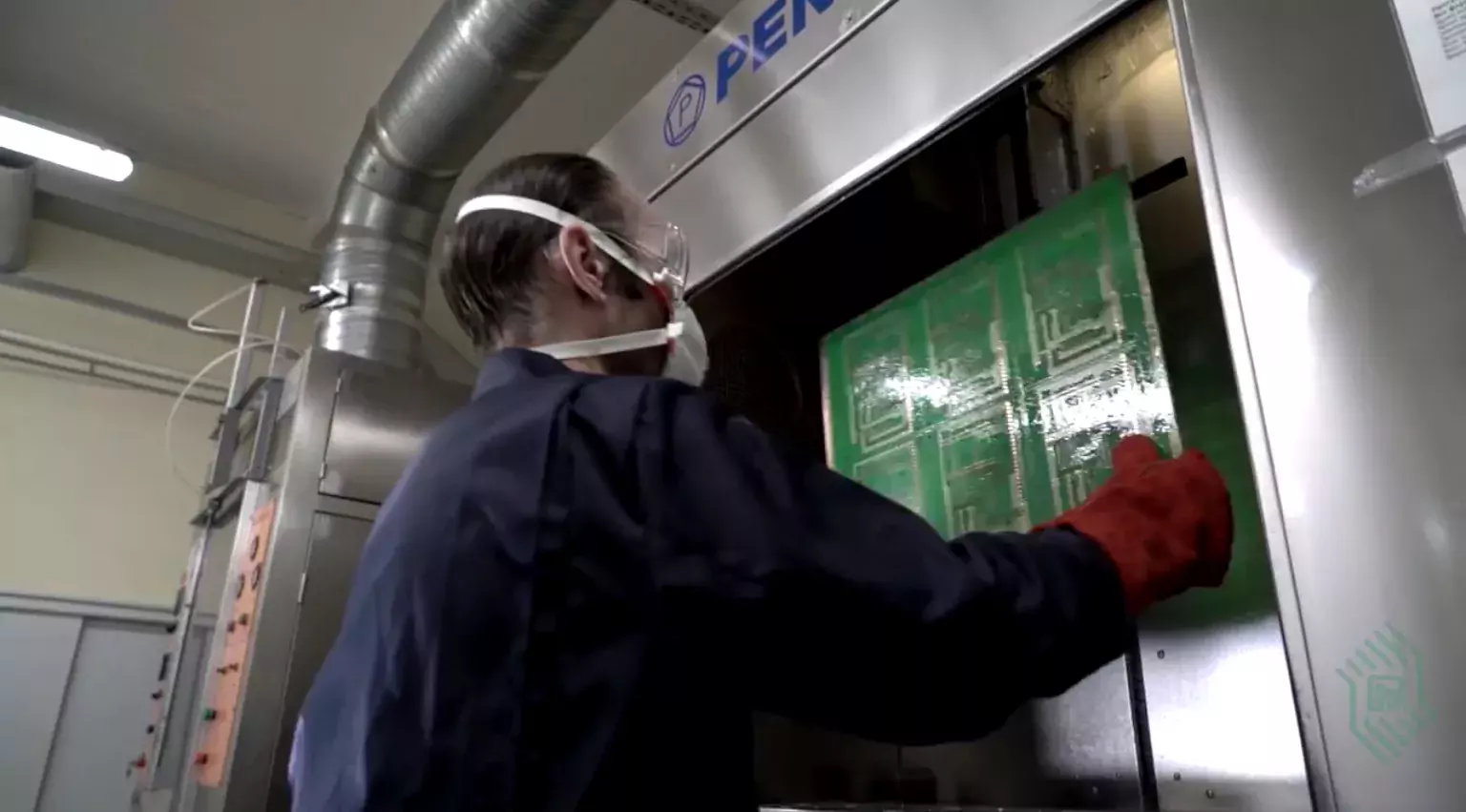
Panel Dipped into Molten Solder Bath
The prepared panel is plunged into a bath of molten solder for a few seconds. The excess solder is then blown off with hot air and a thin even coating remains on the pads.
After cooling the flux residue is washed away.
Today, it is mainly used in military and aerospace applications.
HASL Plated PCB
Advantages:
- Low cost process.
- The shelf life of the PCB panel is increased.
Disadvantages:
- It is not lead-free.
- Not a hassle-free process.
- The surface finish is not flat enough and apparent contours are visible.
- Cannot be used in High Density Interconnect (HDI) structures
- Extremely high temperatures can affect other materials in the PWB
Lead-Free HASL:
The properties and uses of this finish are the same as HASL, except there is virtually no lead in the alloy.
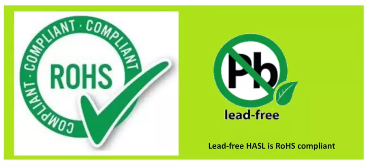
RoHS Compliance
The alloy in place of lead used can be tin and copper, tin and nickel, or tin, copper, nickel and germanium alloy. However, this finish is not widely used.
Advantages:
- Lead-free.
- RoHS compliant.
- Shelf life of the PCB is increased.
Disadvantages:
- The wire bonding is not strong.
- Cannot be used in HDI applications.
Immersion Tin:
The copper pads of the PCB are coated with a tin layer to protect the copper from oxides.
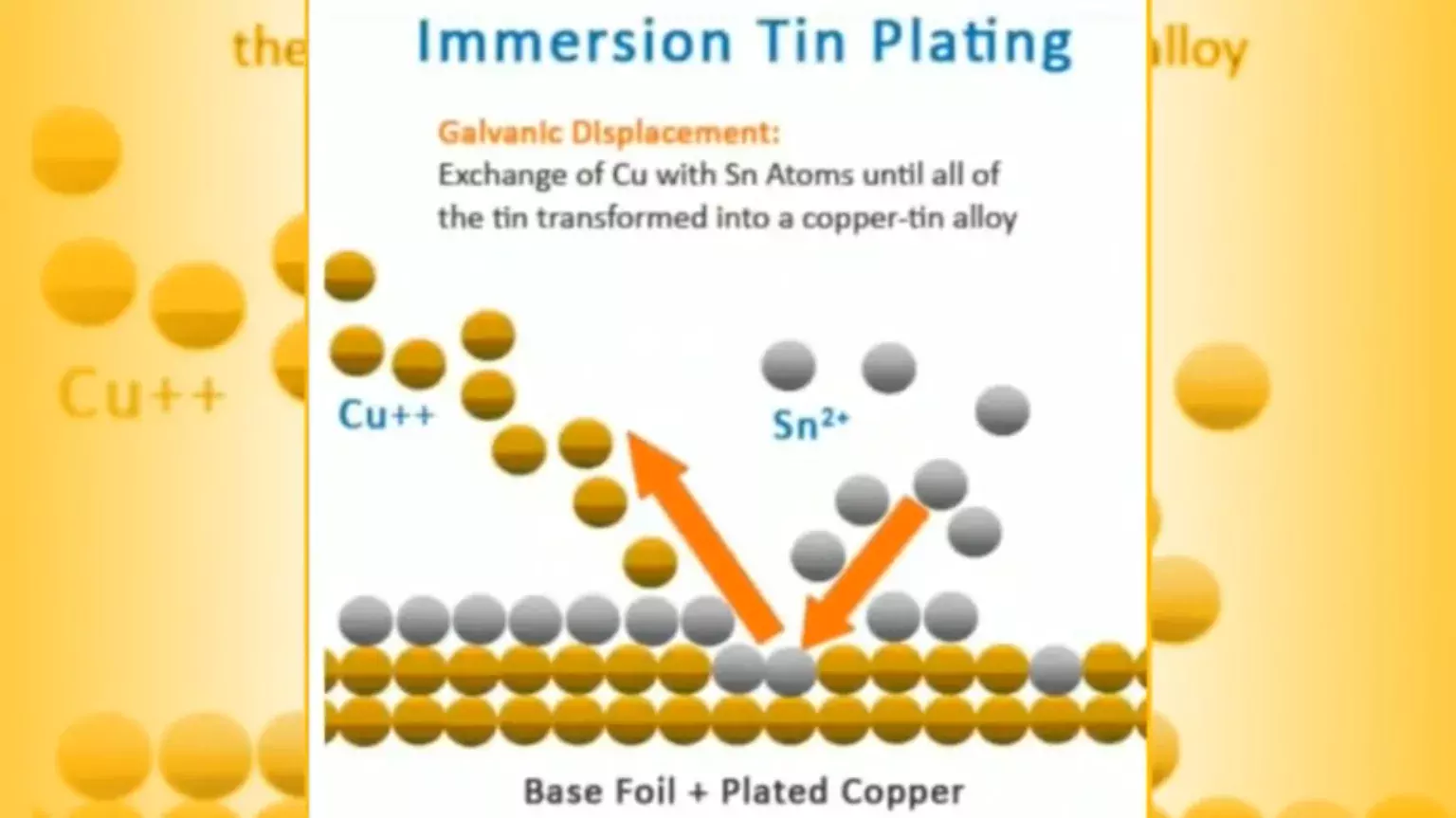
Tin Coating Process
This can be achieved easily by immersing the PCB in an electroless chemical solution.
The layer usually appears whitish therefore this type of surface finish is also called ‘White Tin’.

Immersion Tin Coated PCB
Advantages:
- This is one of the most cost effective methods among immersion surface finishing techniques.
- It is RoHS compliant.
- Provides excellent workable surface when assembling components.
- Used for HDI boards and press-fit applications.
Disadvantages:
- It is not suitable for both sided PCBs.
- It is not suited for a longer storage period.
OSP: Organic Solderability Preservative
Using this method, chemically an organic film is generated which has anti-oxidation and moisture resistance to protect the copper surface from being oxidized.

OSP Coated PCB
It uses a water-based organic compound that selectively binds to copper and protects the copper until soldering.
Advantages:
- Provide flat surface finish.
- RoHS compliant and environment friendly.
- Low cost.
- Wire bonding is strong.
Disadvantages:
- OSP layers are extremely sensitive to handling and can easily get scratches and marks that might affect its solderability.
- Shelf life is also not very long.
- Not available generally with most manufacturers.
Selection of Surface Finish Type: What Suits You Best?
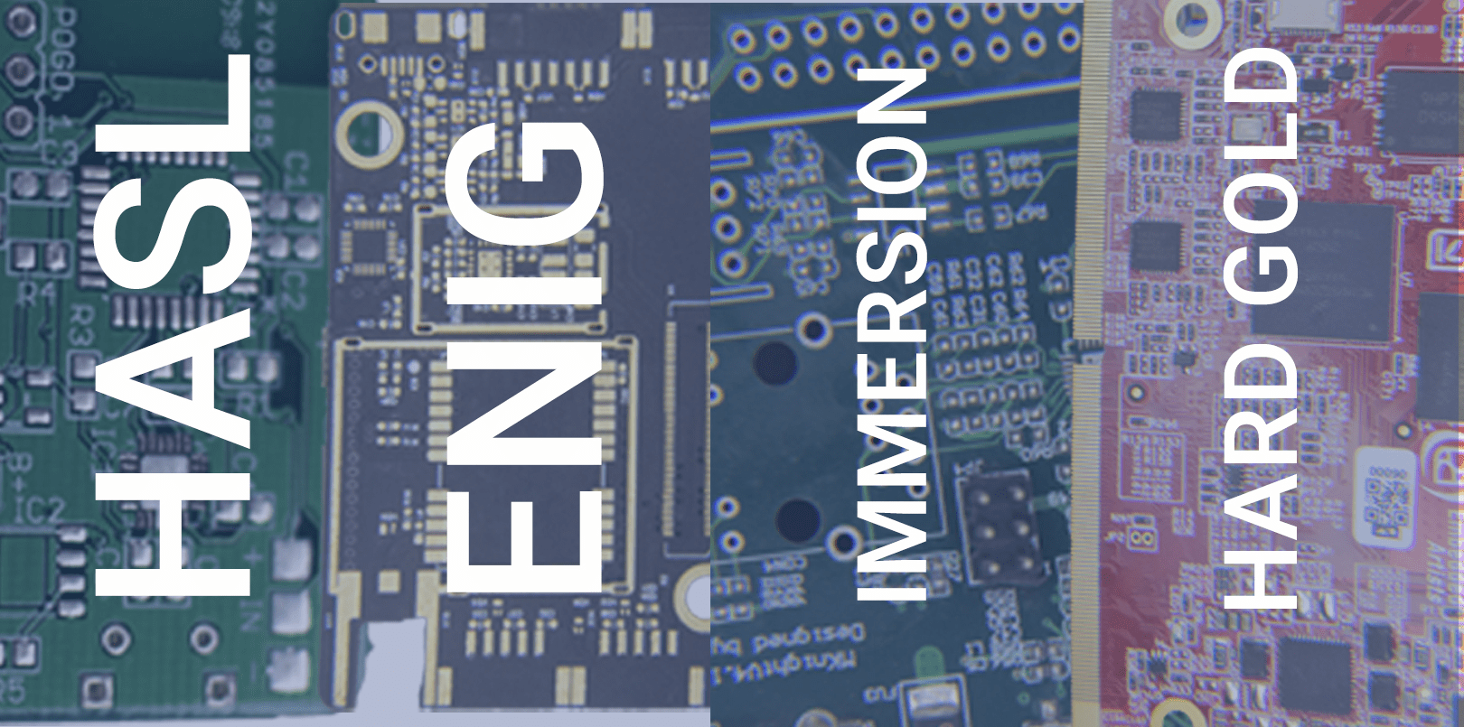
Image from Next PCB
Which surface finish type best suits is choose based on:
Environment in which the board operates, finishing on the surface needed, shock and drop absorption, inter-metallic joint, process yield, rework for production batches, scrap rate, use, board aesthetics, temperature exposure, cost of manufacturing process, shelf life, process handling sensitivity, testing ability, rate of failure during usage, RoHS compliance, wire bonding and corrosion resistance among other factors.
Therefore, based on applicability and other factors suitable surface finish should be chosen, that will optimize your PCB functioning and increases cost effectiveness.


Leave a comment