Printed Circuit board are like a neural path way for electronic devices. If one knows what PCBs are and how important it is for every electronic gadgets. The process of designing is will be much more interesting. But it sometimes takes weeks for a simple PCB to arrive so, in this article we’ll help you learn to manufacture your own PCB.
Prerequisites
If you have learnt PCB designing, now is the time to bring your design to life. If not learn now from DIY PCB at Learn How To Design A PCB Today!
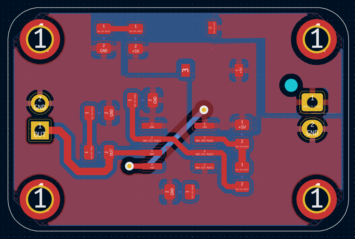
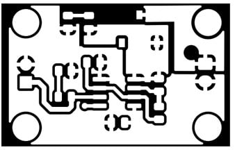
The PCB printing begins when you complete your PCB layout and ensure DRC(design rule check) is done. Since different designer/company use different PCB CAD it hard for manufacture to convert all of them. So, most of the the final design is converted into a Gerber file.
A Gerber file is a collection of different files containing design information of various layers of a PCB. Circuit board elements like copper traces, vias, pads, solder masks and silkscreen images are all represented and defined by a set of vector coordinates. The result of Gerber files will be same independent of software used for PCB designing. These are essential files required by the manufacturer for the manufacturing process.
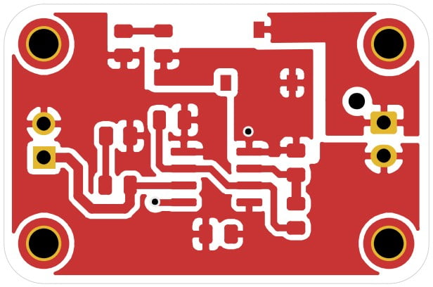
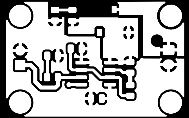
Copper Layer
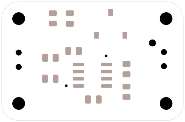
Solder Paste Layer
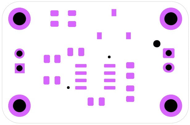
Solder Mask Layer
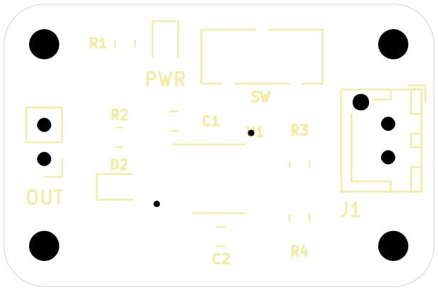
Silk Layer
Above images represent copper layer, solder paste layer, solder mask layer and silkscreen layers of the same design. All the layers are printed on a transparency film which are used as a mask for the photosensitive transfer process.
These are the file extension for each layer inside the the Gerber folder:
| File Extension | Layer |
|---|---|
| filename.GTL | Top Copper Layer |
| filename.GBL | Bottom Copper Layer |
| filename.GTS | Top SolderMask |
| filename.GBS | Bottom SolderMask |
| filename.GTO | Top SilkScreen |
| filename.GBO | Bottom SilkScreen |
| filename.GKO | Board Outline |
| filename.DRD | Drills |
File Preparation
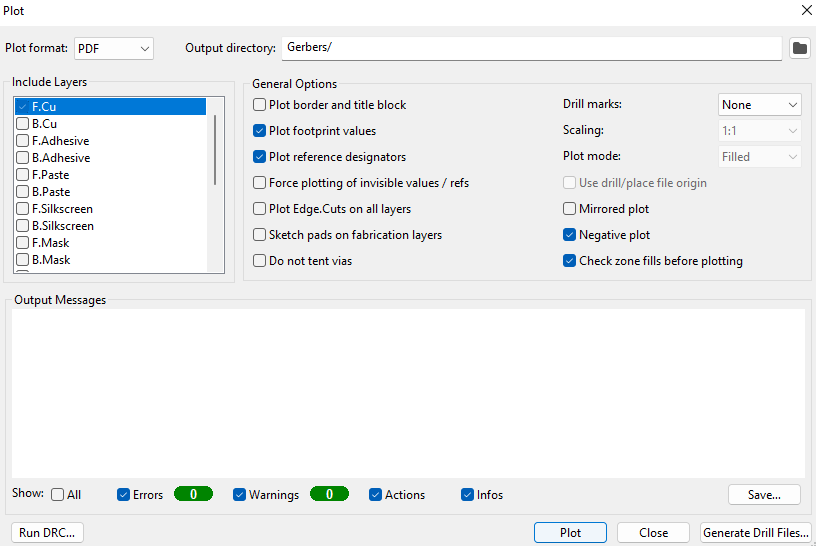
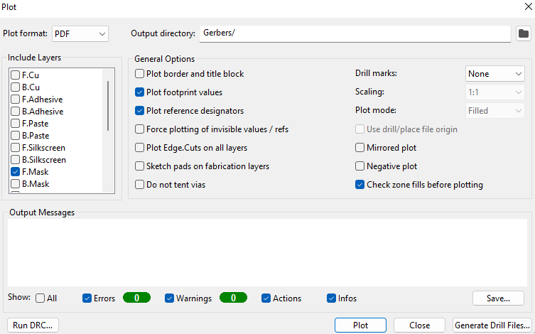
In this article we will be keeping things simple for you as a beginner and we’ll only learn manufacturing a single-layered PCB. Thus, while exporting your PCB design from software, export a PDF file with inverted copper tracks to print on a OHP(Overhead Projector) sheet. We’ll talk about why the copper track is inverted in the further steps.
If you are using KiCad you can follow the below setting on your plotting option to get the Inverted copper trace on a PDF file.
You can watch this video for more details :
If you like to test a pre-existing Gerber, use our Gerber Viewer!
Material Required
(Affiliate Links)
- Copper Clad : https://amzn.to/3RmU96h
- Transparent OHP Sheet : https://amzn.to/3KQ6Vbb
- Dry Photo Resist Film : https://amzn.to/3RmUC8x
- Laser printer 600dpi or greater : https://amzn.to/3KV0vY5
- Iron or Laminator : https://amzn.to/3TMJ6oB
- Ferric Chloride : https://amzn.to/3D9GjAd
- Sodium Hydroxide or Pure Acetone : https://amzn.to/3qjb8L0
- UV curable solder mask : https://amzn.to/3Qi7pIh
- Gloves : https://amzn.to/3euSMUt
Manufacturing
File to Film
Print the photo negative of the PCB layout which we prepared earlier on to the OHP sheet. To keep the print perfect, use a Laser printer to print the layout onto the OHP sheet. This would reduce the smudging of the ink and keep the layout perfect.
Print the copper track to OHP sheet
Here the black part of the image will make the copper clad unexposed on UV light and gets copper etched away during the etching process and gives the required tracks and pads on the copper clad.
Film to Board
There are multiple ways to transfer the PCB layout into the copper clad. We can either use the tone transfer method or UV photo resists method. In this article we’ll be use the latter.
Peel the protective lamination from the dry filmphoto-resist and stick it our FR4 (Copper clad)board. This photo-resist comprises a layer of photo reactive chemicals that harden after exposure to ultraviolet light. This harden surface will prevent the copper with circuit getting etched away.
Tip : To stick the dry filmphoto-resist firmly on the copper clad, gently iron over the photoresist or cut the copper clad into a smaller section and pass it through a laminator to ensures the photoresist adhere onto the copper layer
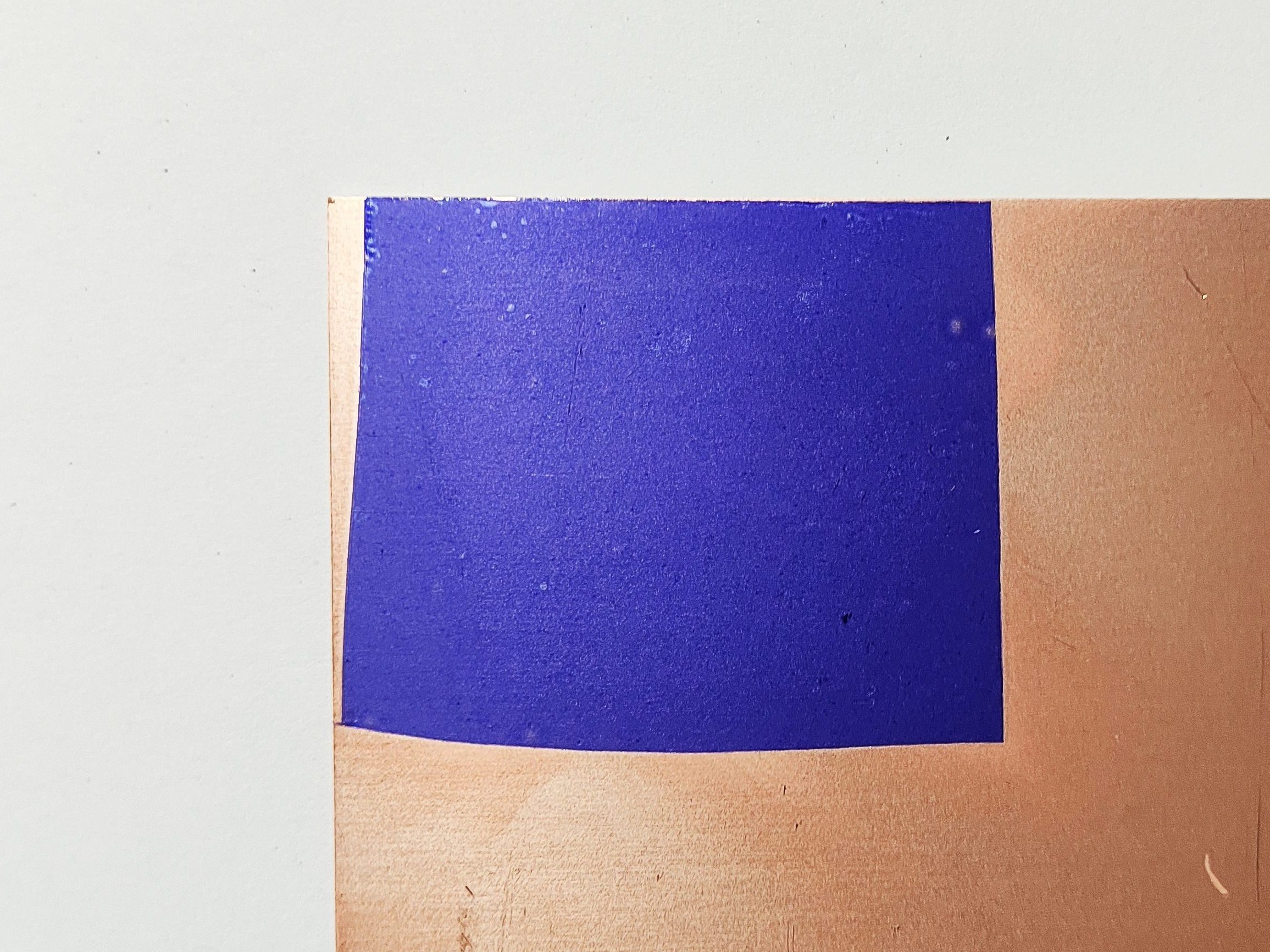
Photo- resist layer on FR4 board
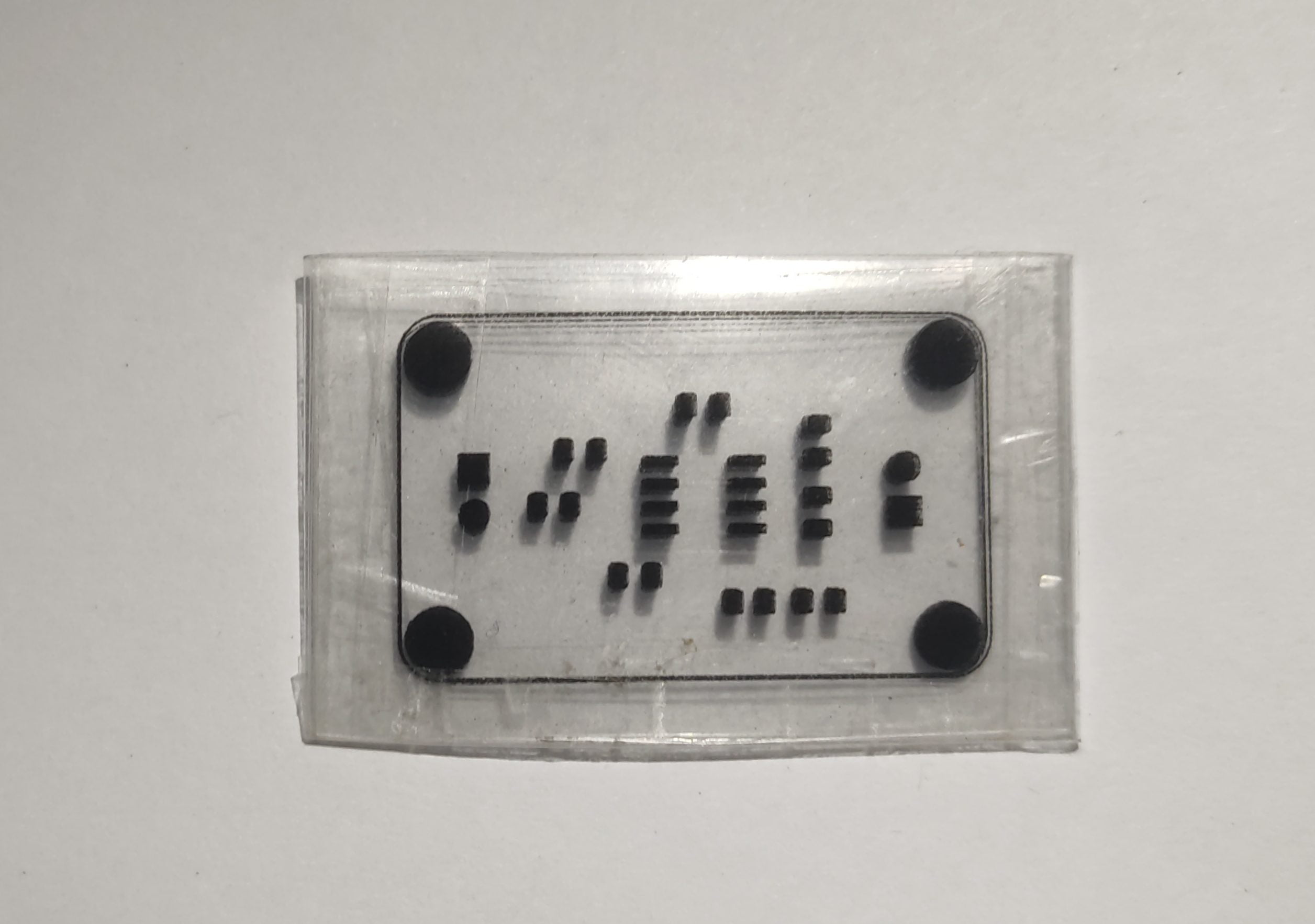
Now to transfer the circuit to the board, place the OHP sheet from the previous step on to the top of the dry filmphoto-resist copper clad. This we’ll help in not exposing the copper parts that’s not part of the circuit, so it can be etched away easily later.
OHP on FR4 board
Tip : If the print (black colored traces) looks translucent, then take multiple copies and sandwich them to make it more opaque
Place the printed mask on to the photoresist and expose board to UV light to transfer the imprint. Alternatively it can also be exposed to sunlight or halogen lamps. The exposure time depends on the type of the source used. UV LEDs produce the fastest results and reduces the time to minutes. Halogen lamps require prolonged exposure times. Overall it takes a few trials to find out the perfect exposure time for the source that you are using.
Excess Photoresist Removal and Visual Inspection
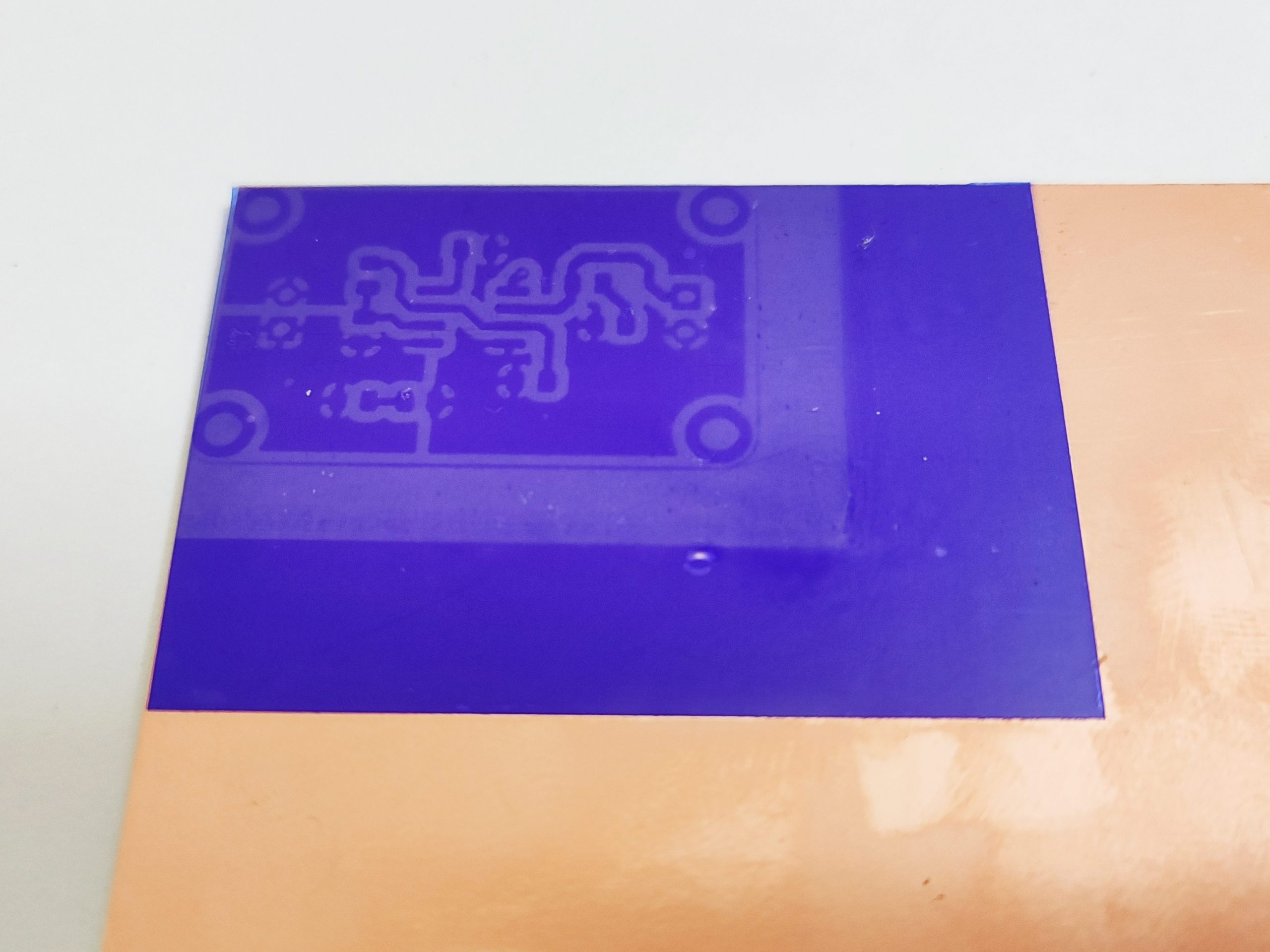
Photo- resist layer after exposing to UV source
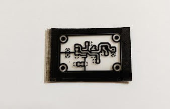
Once the UV exposing is done peel off the OHP film from the exposed photoresist. You can see the exposed parts turn to darker shade than the unexposed photoresist. Also the exact circuit pattern from the OHP is transferred on the photoresist layer. Now the unexposed areas can be removed using an alkaline solution like sodium carbonate or anything equivalent can be used to dissolve the unexposed photoresist.
Immerse the PCB in the alkaline bath for few minutes and gently rub it with smooth hands or a brush to remove the mask.
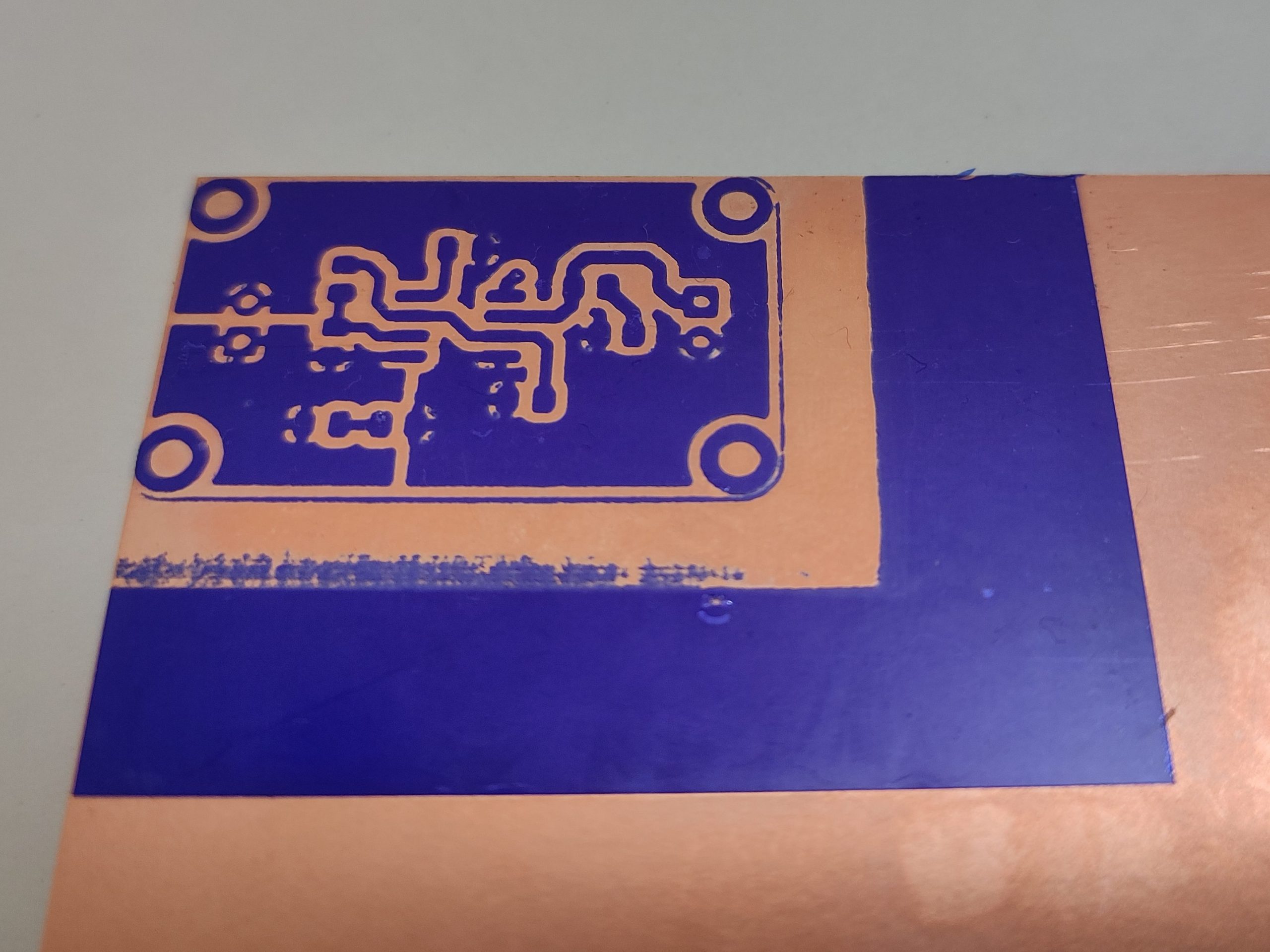
Photo- resist layer after alkaline cleaning
The board now glistens with only the copper substrate necessary for the PCB. Now before moving ahead, make sure to have proper visual inspection check whether the traces are still imprinted perfectly. Any cracks or defects on traces can cause functional flaws later in your PCB board.
Copper Etching
Any unwanted copper is removed using any copper solvent, in this case we use ferric chloride. Make a solution of ferric Chloride by dissolving it in water. Immerse the board in it for 10-20 min which is enough for dissolving any unwanted copper.
Tip : Ferric Chloride dilution must be moderate (Most of the time mentioned on the package). If the solution is concentrated, it will etch away too much copper. If the solution is very diluted, the time required to etch the copper will be greater.

Ferric Chloride Bath
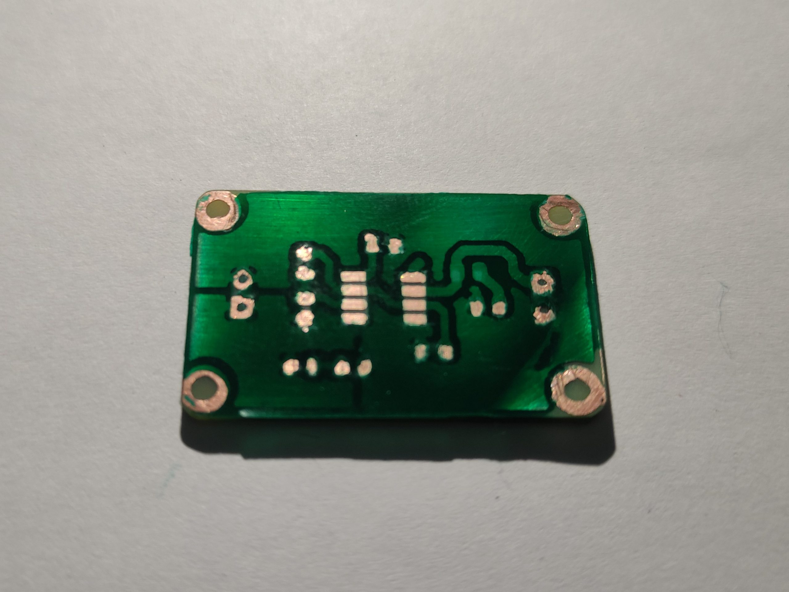
Thus through this process, the copper from uncovered areas is completely removed. Wash the board in plane water.
After removal of excess photo-resist imprint
Now using sodium hydroxide (NaOH) solution, remove the photo-resist imprint on the board. This process is very slow and we have to rub the photo-resist from time to time.
After Removal of excess copper
By inspecting the board ensure that none of the traces are washed off and if it looks fine, your PCB manufacturing is complete.
Surface Finish
The surface finish forms a critical interface between the component and the PCB. The finish has two essential functions, to protect the exposed copper circuitry and to provide a solderable surface when assembling (soldering) the components to the printed circuit board. There are various kinds of surface finishing techniques used by the manufacturers and most of them are done industrially, so manufacturing PCB at home you can skip this step.
However, it’s an important industrial step so its better know about them. The various kinds of surface finishing techniques are:
- Hot Air Solder Level (HASL)
- Lead-Free HASL
- Organic Solderability Preservative (OSP)
- Immersion Silver (Au)
- Immersion Tin (Sn)
- Electroless Nickel Immersion Gold (ENIG)
- Electroless Nickel Electroless Palladium Immersion Gold (ENEPIG)
- Electrolytic Wire Bondable Gold
- Electrolytic Hard Gold
Adding Solder Mask
Though ideally PCB manufacturing is complete, if you leave your copper board exposed to the atmosphere as it is, it will soon start oxidant. To prevent oxidation of copper board, manufacturers colour code their PCB which is called solder mask.
Just like how we generated a Geber file for the PCB design
Solder Mask Layer
Below image shows an example how to export solder mask using KiCad plotter function.
KiCad Solder Mask Layer Export
Using a laser printer take a print of solder mask on the OHP sheet, just like the earlier process.
Solder Mask Layer on OHP sheet
For the solder mask we’ll be using UV Curable Solder Mask, which will work similar to the dry photoresist film.
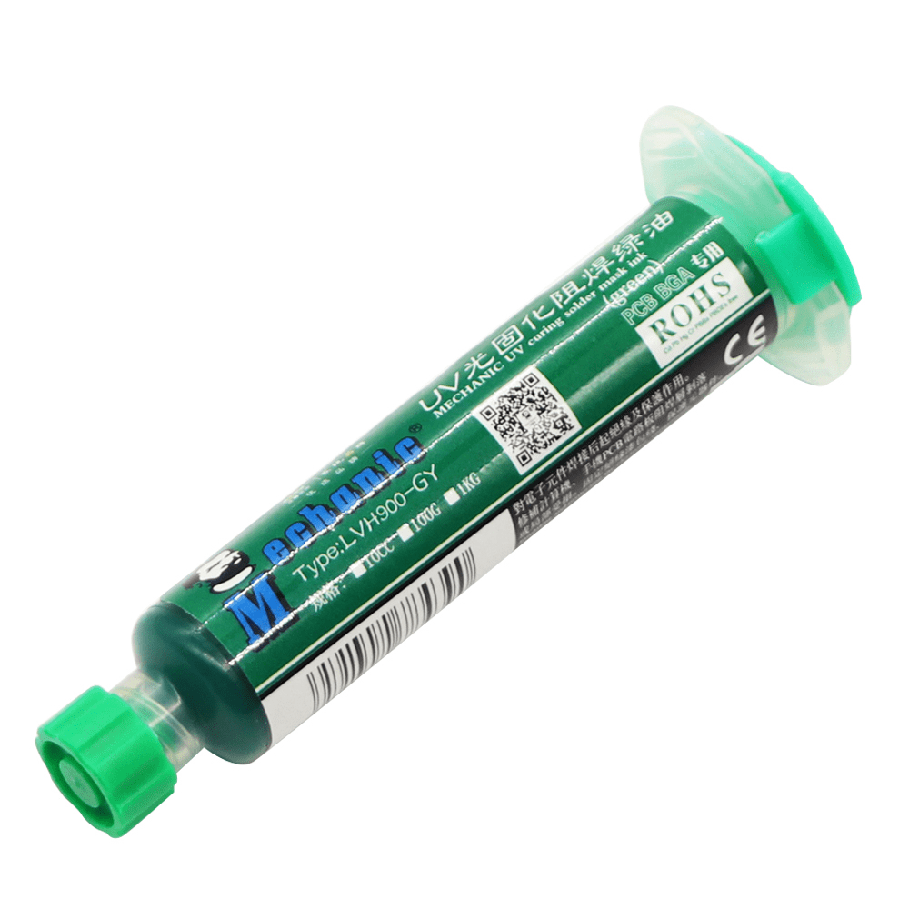
UV Curable Solder Mask
Place a blob of UV curable solder mask and cover it with a piece of transparent film. Spread the UV ink evenly with a help for a flat plate or a glass sheet.
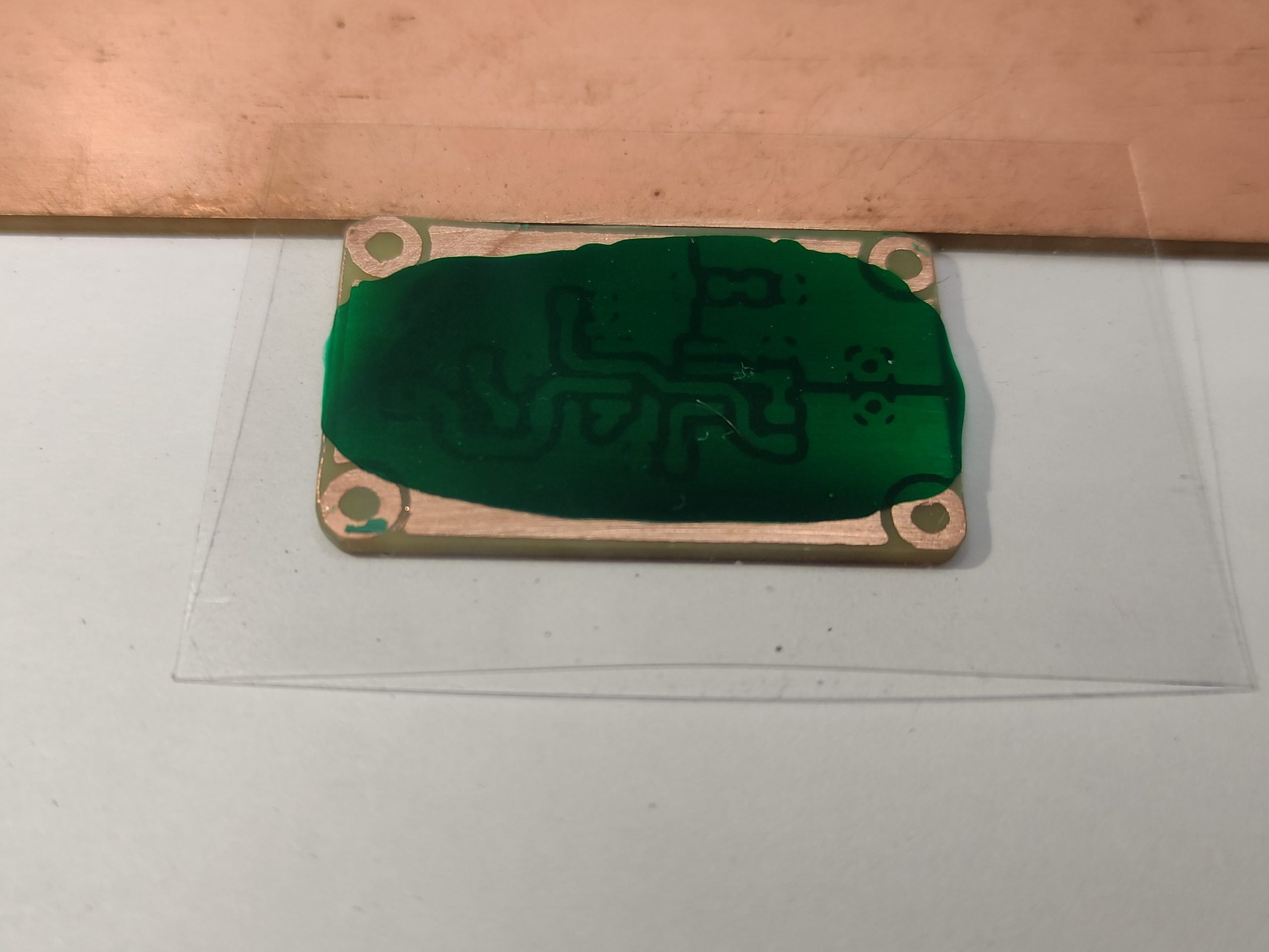
Applying Solder Mask
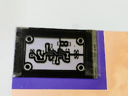
Align the printed mask on the PCB and place it under a UV lamp for exposure. Similar to the previous steps this process take a few trials to find the correct exposure time as it also depends on the consistency of the UV ink that’s spread over the copper clad.
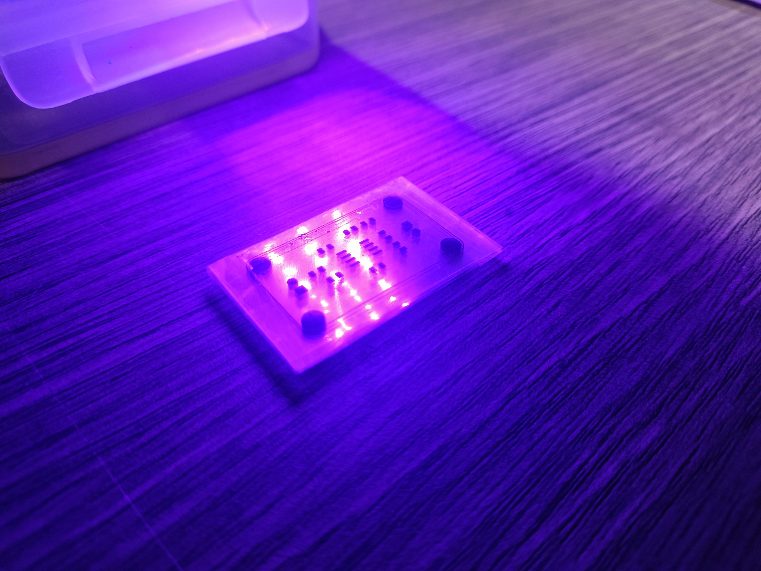
Exposure to UV light
Finally after the UV curing remove the unreacted ink with solution of acetone or Isopropyl alcohol.
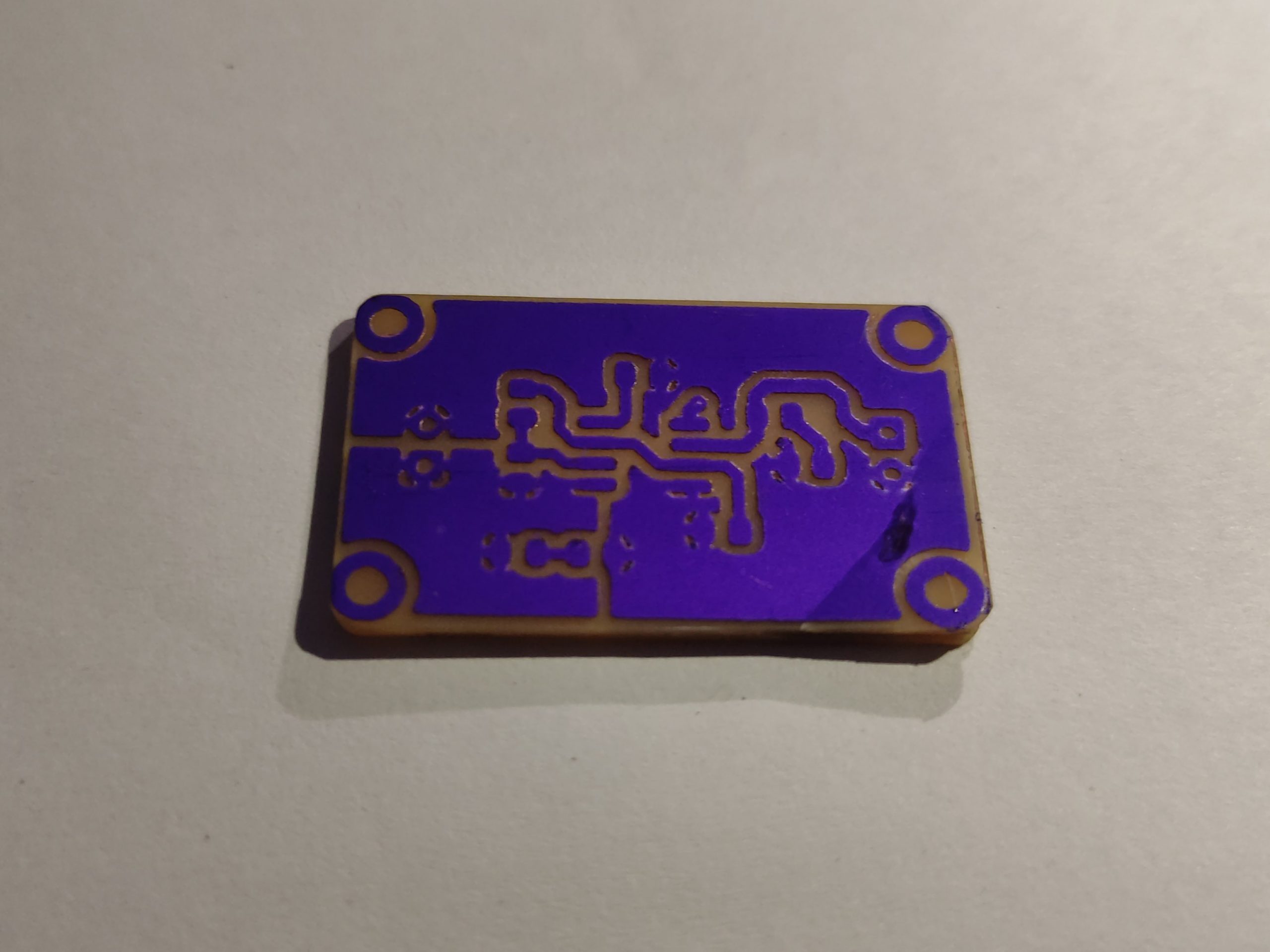
After Acetone Bath
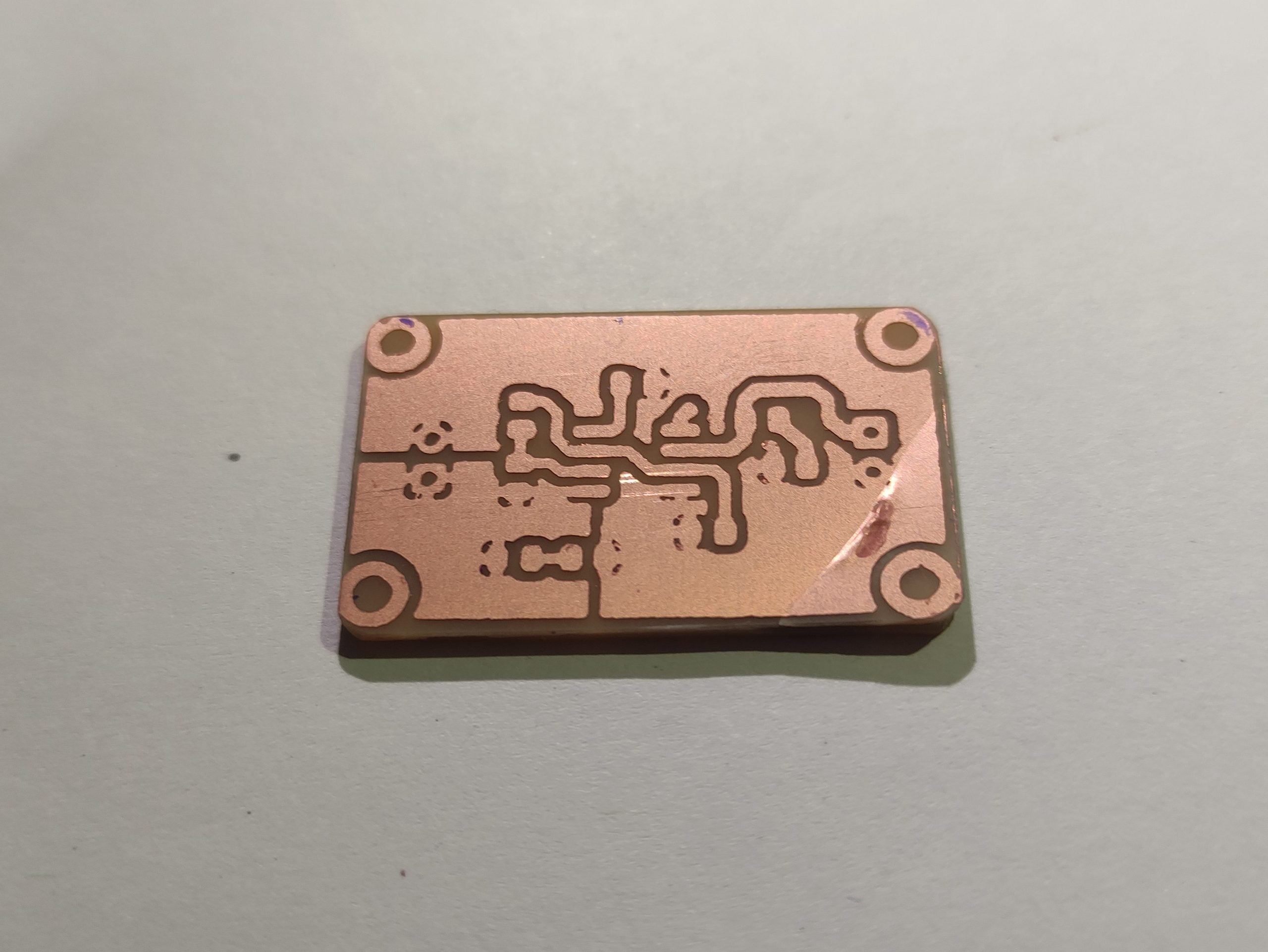
This completes your professional style PCB manufacturing at home with solder mask on it. This is no means the perfect Printed Circuit Board, You can see inconsistent solder mask over the copper clad. Also there is no silk layer to give the designation to different component on top of the PCB. But this is a great starting point for a DIY PCB manufacturing at home.

Silk screening
If you need a silkscreen, You might need to additionally invest in printing screen and silk layer paste which can increase the cost exponentially for somebody just getting started. That’s the reason we skipped the process of using screen printing and adding silk layer.
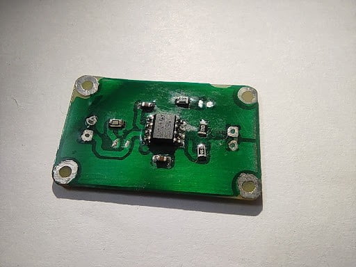
Assembly
The only thing left now is to assemble and test the PCB just fabricated. In case if your PCB contains through hole components you might also need to drill them with necessary diameter for those components.
You can learn both process here : Assembly and Testing
The feeling of accomplishment that comes with doing the hard work and manufacturing one’s own PCB from scratch is eternal! Even though the PCB is *Bleh*, with few more tries and with more experience many have come up with great results.
This manufacturing experience evolves your understanding about PCB as a whole. You understand the dynamics of various layers that goes into making a single board of PCB. You can always keep us posted with your progress or any further queries.

Leave a comment