
Printed Circuit Boards are lifeline of electronic world. PCBs make our job easier by eliminating wiring in traditional circuits or breadboards. Since PCB is the carrier of the entire logical circuit, the first and foremost job of any designer is to curate a PCB design before manufacturing.
PCB Board Design
If you are really interested in getting into electronics design, designing your own PCB from scratch all by yourself must have been one of the priorities on your to-do list. Here we’re going to provide you a step-by-step guide to help you manufacture your own PCB from idea to schematics to manufacturing. Also we won’t be using any specific design software, instead this guide will be generic and will help you understand the basics and apply it on any design tool.
Draw Schematic
Logical and visual representation of an electrical circuit is called a schematic diagram. It is the very first step of electronic product design. Before you start drawing your schematic on the software it’s important to be clear of your design and have a rough layout of the circuit. For this, you can divide your circuit into small logic block which will help you see the big picture when you are building your schematic.
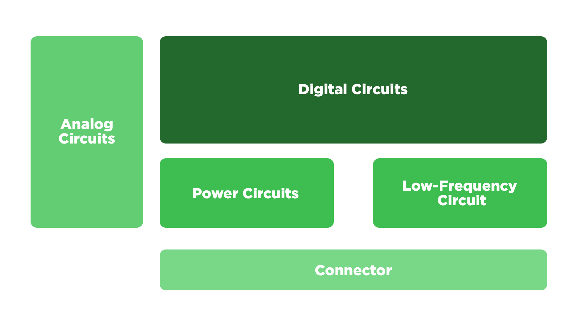
Block diagram of a circuit
Today, designers use numerous EDA (electronic design automation) tools such as Altium, Allegro, Pads, Kicad, Tinycad, Express PCB, and so on to draw the schematics which earlier were done merely on papers. These design tools ensure that the schematic circuits are error-free as they continually monitor logical and connection errors. We’ll soon make a guide to help you choose the right design tool for your use case.
Draw your schematics using PCB Software:
Humans are prone to errors and easy to make mistake and mistake in PCB design can cost money and man power to fix. So Designers need to follow a standard design rule to make the schematics machine-readable and easy to understand. A good schematic shows a well-structured circuit diagram clearly depicting the electrical connections between various electronic components which is easy to understand at a glance.
Note: A technically correct but crowded schematic is still a bad one as it might confuse other engineers, so avoid chaotic layout.
Chaotic Layout
Good Layout (Can be better)
No matter which PCB software you use there is a flow to the schematic designing:
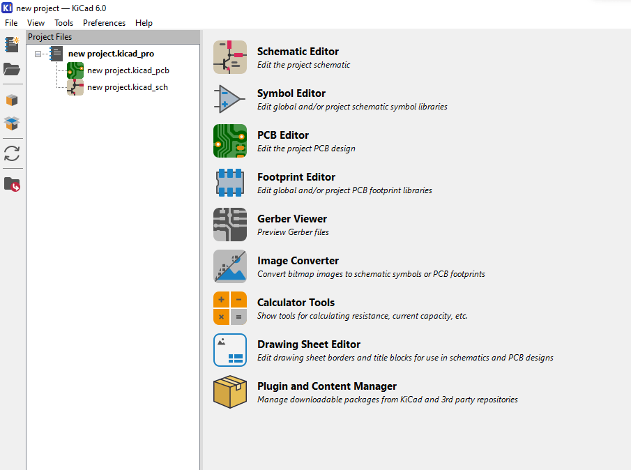
- Create a new Project:
In case you use EAGLE, in the control panel, under Project tree within an eagle directory create a new project. In case if you use Altium Designer, add a new project from “Add new project” directory within Project tree. If love open source and use KiCAD, add a new project from the file menu and open the schematic Editor
KiCad interface
- Adding parts to your schematic:
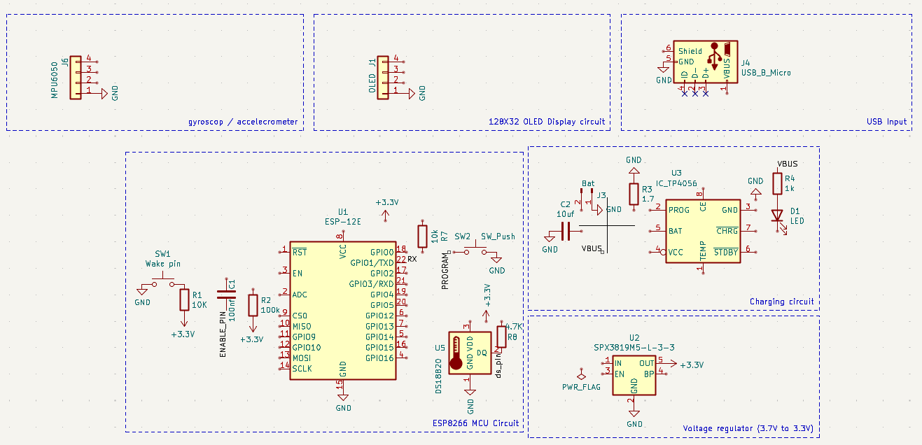
- Adding Major circuitry – First start with placing most crucial components of the circuit, like microcontrollers, logical units, amplifier IC or any other important part of the circuit.
- Adding Supporting circuitry – add other components like resistors, diodes, capacitor or other little complex circuits like filters, rectifiers, etc. Which might be required by the major circuitry.
- Adding connectors– depending on your design choose the connectors you need. For instance, Male header pin, Female header pin, JST connectors which can help in connecting to different circuit.
- Adding Power Input– Connect appropriate power to the Major and Supporting circuitry
- Add a frame or a block – though this isn’t a critical component of your schematic layout but it keeps your schematic look organized and also helps in keeping them as logical units for better understanding.
Note : Drawing a schematic can be complicated, if you are using rare parts or newer parts because the availability of the symbol (component) within the design software in unknown. So in some case the symbols have to be custom made (Where this process varies from software to software).
Components Placement
- Wiring up the parts on schematic:
With this your schematic is complete in terms of putting every component. All it needs now is to wire these parts together.
- Names and value labelling of your schematic:
Every component on your schematic should have two editable text fields: a name and a value.
The name is an identifier like R1, R2, LED1, etc. Every component should have a unique name. On other hand, the value allows you to define unique characteristics of the part. For eg, a resistor’s resistance or a capacitor’s capacitance.
While there can be numerous more steps and functions a designer can follow on any of the PCB design software, as a beginner we should stick to the basics and slowly get into the complications of the software. For instance, you can have logical blocks of your schematics on separate pages, each page dedicated to block diagrams, power supply, MCU interference, revision history and so on.

Final Schematic
Pre-requisites
Once the designing is complete, it’s time to convert that schematic into a PCB. For this a PCB layout is to be designed based on your schematic and according to the number of holes, pads, traces necessary, location of components, etc.
However, before this few pre-requisites should be fulfilled.
First we initiate the design of stack-up and ensure that the BOM is verified for all parts and all parts are active.
BOM (Bill of Material) is the list of required PCB materials for manufacturing, this is done to ensure that all the required materials are available. Thus, following verifications is to be made-
- Manufacturing Part Numbers (MPN)
- Vendor Part Numbers (VPN) are correct
- The quantity of the parts is correct
- Designators match the schematic
- DNI (do not install) components are marked in BOM
Finally PCB stack up design is done using following parameters-
- The material of PCB (FR4, Rogers, etc.) depending on the operations and environment.
- Number of layers, both- signal layers and power layers.
- Impedances required (Doesn’t matter much for simpler board)
- The thickness of copper
Component Selection
An important decision here is what mounting technology you should choose for the components Through-hole or surface mount?
Through Hole technology (THT) is a method for constructing electronic circuits in which the pin-through hole (PTH) components are inserted through holes drilled into PCB. The ends, or leads, are then affixed to pads on the opposite side with molten metal solder using wave soldering or re-flow soldering equipment.
THT bonds are far stronger than SMT bonds, making THT the ideal choice for components that will be subjected to mechanical and environmental stress or high heat, such as connectors and transformers. THT components are also simple to swap out, making them ideal for prototyping and testing.
It does have some disadvantage which led to the development of SMT, THT component leads must be fed through the board, the PCBs must be pre-drilled, which is both costly and time-consuming. Because the holes must be drilled through all of the PCB’s layers, it also confines components to one side of the board and limits the available routing area on multilayer boards. THT soldering frequently produces less reliable solder points than SMT solder. Furthermore, THT assembly is more involved and thus more expensive than SMT.
SMT or Surface mount technology is a frequently used assembly process in the electronics industry. In this technology, electronic components are assembled with automated machines that place components on the surface of a board. In contrast to the procedures involved in the conventional through-hole technology (THT), SMT components are placed directly on the surface of a PCB instead of being soldered to a wire lead.
SMT can be used on both sides of the board and at higher densities, enabling smaller, more powerful PCBs. Because no holes must be drilled, bare board costs are lower and production times are faster. SMT components are up to ten times faster to place than THT components. In soldering process, the solder is much more reliable and can be applied quickly and evenly. SMT has also been shown to be more stable and perform better in shake and vibration environments.
The main disadvantage of SMT is that it can be unreliable when used as the sole attachment method for components that are subjected to mechanical and environmental stress as well as high heat.
The answer to the question of through-hole vs. surface mount technology is to combine the two. It all comes down to use cases and how the board is processed during assembly, providing the strength and reliability of THT where needed while retaining the overall cost and efficiency benefits of SMT.
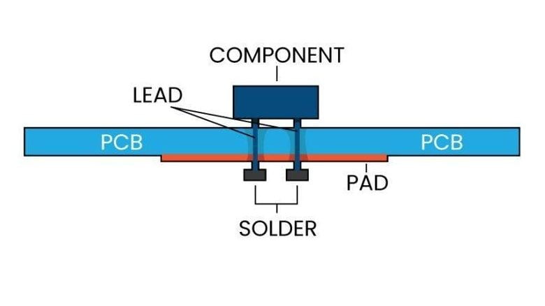
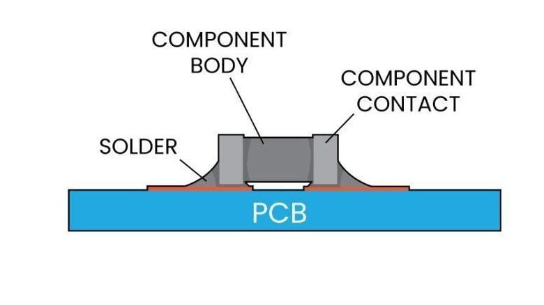
Footprint Assignment
Footprint is the arrangement of plated pads where a component is supposed to be soldered. It is also called the land/pad pattern and resembles the physical dimensions of the component. This footprint connects a component to the circuit board both physically and electrically. It gives an idea about the component placement and the trace locations.
Similar to symbol in schematics, the footprint might not be available for your part within the design software, in that case they have to be custom made.
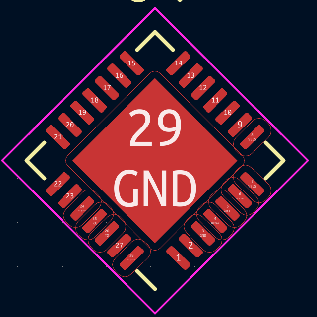
Footprint
In some case(some design software) footprint are auto assigned to the symbol when the schematic is drawn. If not they have to be manually done.
Design Board Layout
Once pre-requirements of BOM, Footprint assignment and stack-up design are fulfilled it’s time to start with PCB board layout.
Following steps are to be followed:-
- Setting up the stack-up: A single layer stack-up by default is defined when we start. Further new layers can be added using Add Stack/Layers. Multiple layers can be added depending on the complexity.
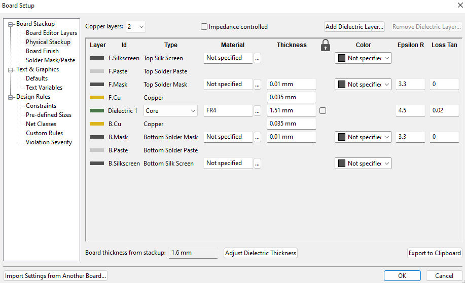
Kicad Physical Stackup
- Refer to PCB fabrication notes: These are the notes which have be referred from your manufacturer to make sure you adhere to there capabilities. This includes information like- class of PCB, overall board thickness, IPC standards, colour of solder mask available, silkscreen, layer wise impedance details, cut-out details, stack-up details, drill-hole chart and version number and date.
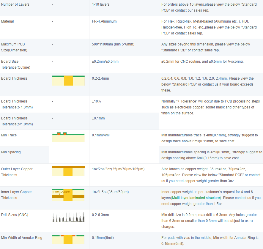
Manufacturer Capabilities
- Set the PCB design rules: These are the design rules that we setup before starting the board design, this includes setting up clearance between traces, trace width, copper fill zones etc. Skipping this stage would make the board design development cumbersome when the complexity is increased. Broadly they are classified rules that we have to consider – Electrical design rules, physical design rules and spacing design rules. This process will require you to go back and forth between previous step and this step.
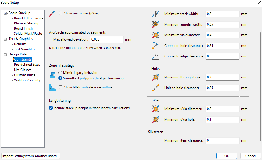
Kicad Design Rules Setup
- Draw the PCB outline: A closed contour is essential where all the components are placed within the outline. In Kicad this is called as Edge cut layer which defines the shape of the board. In case you have complicated board shape, it can be imported from different CAD tool.

Board Outline
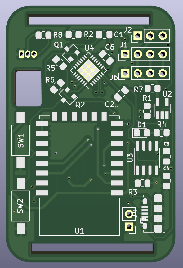
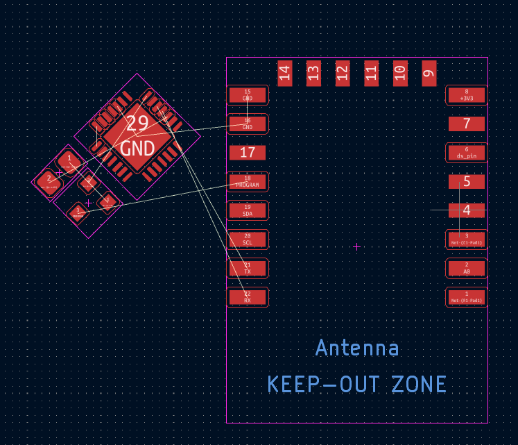
- Component placement: This step is similar to schematic design guideline but the board layout is converted into a physical object, there are more fundamentals rules that you can follow to decrease the chance of failure during production. You can referee to our article: 7 PCB design guidelines professionals won’t share.
- Cross-select mode: This is not a essential step but will definitely help in speed up the board design. This basically means that if you select an object on the layout the corresponding object on the schematic is also selected, thus making the component placement accurate. Some of the design software have them turned on by default, but on few we might have to manually turn on this feature. Tip : Having a dual monitor will greatly speed up the process.

Manually turn on cross selection
- Route the Rat nets: This is the process of laying copper traces between the nodes. Interactive routing can be easily done with the modern EDA (Rat nets are the thin lines that show that connection between 2 points). Once routing is complete, ground places are added to the PCB layout.
Ratsnest
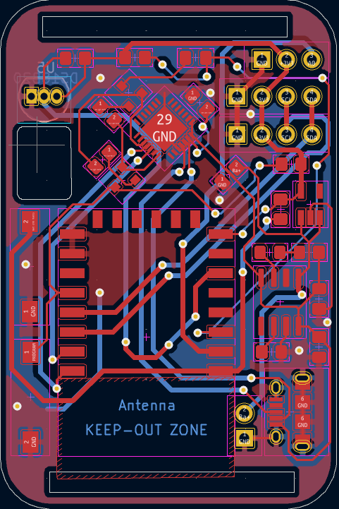
Routed PCB
- Time for Design Rule Check (DRC): This is be done to check if all the connections are done properly and if we have followed the design rules that we setup in the initial phase of the board layout design.
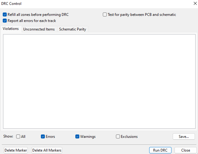
Kicad Design Rule Check
Once you are done board layout designing, do Design Rule Check (DRC) to encounter any error. If you find any error, follow up the error message and fix the issue before going to the next step.
Gerber File Generation
Gerber files play an important role as a connector and translator between PCB design engineers and PCB manufacturers, allowing manufacturers to understand design engineers’ considerations and concepts so that correct and reliable products can be effectively and efficiently manufactured.
Gerber files generally contain design data of conductor layer, solder mask layer and silkscreen layer. Different PCB design software feature different operation steps of Gerber files generation, so depending on the type of design tool you use the generation method may vary.
Send PCB for Manufacturing
Once the designing is complete and Gerber file is generated, it’s time to get your PCB design manufactured. There are many manufacturers available online whom one can contact and they will manufacture your PCB based on your schematic design. However, one can also manufacture them at home if you plan on doing a simpler design, for which you can refer to our article How to manufacture PCB at home.
Just manufacturing won’t complete the process of PCB development, there are few more additional stages that required to complete the development process (like fly probe testing, Components Assembly, functional test, etc) which we’ll see in the upcoming articles.
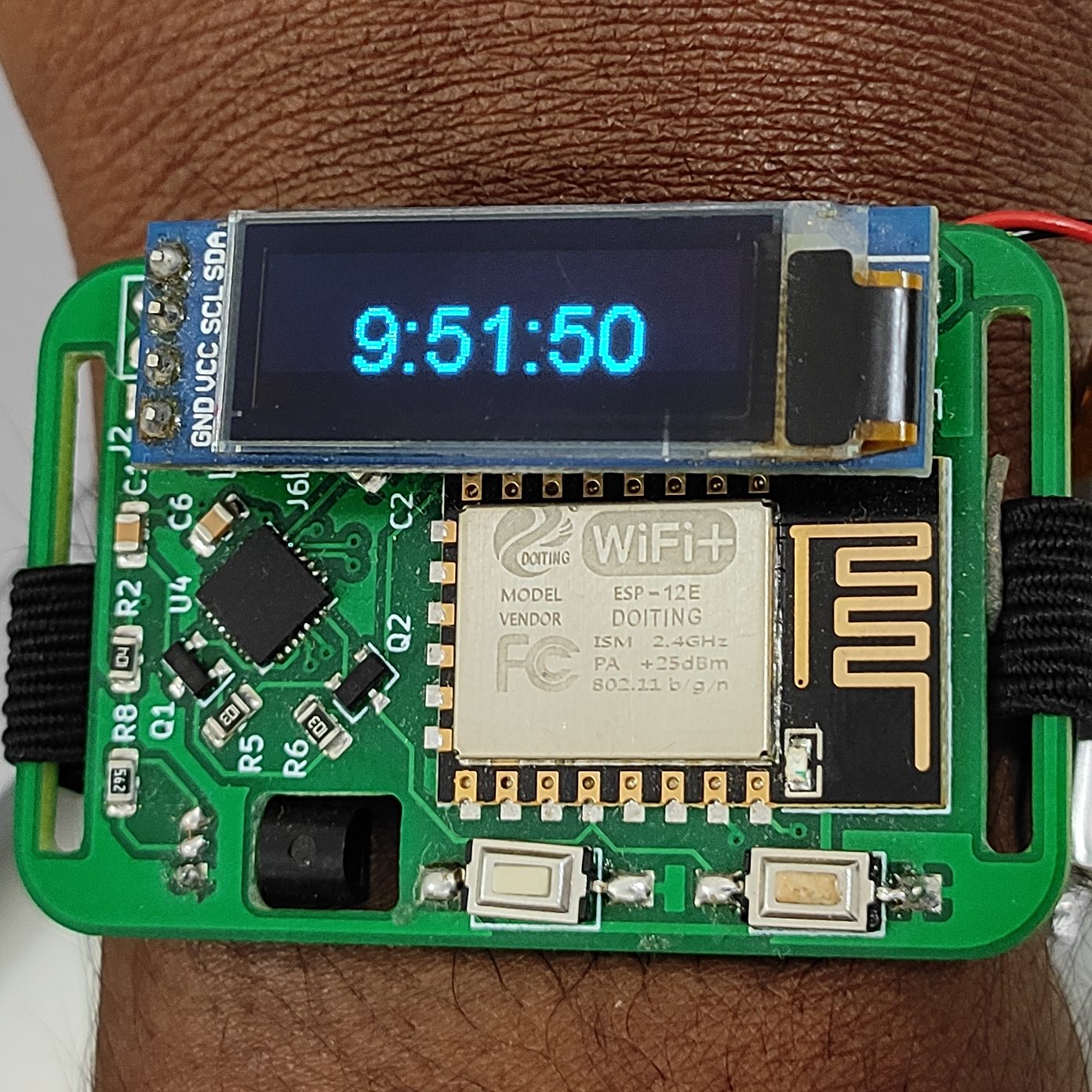
Manufactured PCB
PCB development is a iterative process, it’s very hard to get it right on first try. Just like every skill with practice and consistency, you’ll evolve your PCB designing skill. Also, if you fail at your first PCB, repeat until you achieve the desired result and don’t be disheartened. Always remember what Thomas A. Edison had said, “I have not failed. I have discovered 10,000 ways that won’t work”.
If you have just stumbled across this article and want to know what is PCB check this article What is PCB?


Leave a comment