![What and Why do we need PCB? [Because Size Matters]](https://pcbcupid.com/wp-content/uploads/2022/07/PCB-Cupid-Article-1_IMG_020822.png)
To light a bulb an electric wire is required. Now imagine how many wires will be required to light an entire LED screen of your phone? And also, inducting these wires to a common circuit that has n numbers of other wires connecting speakers, camera, microphone, button of your phone? If you imagined right, you won’t be putting your phone in your pocket but will be needing a whole dedicated bag for your phone with its mesh of wires and circuits.
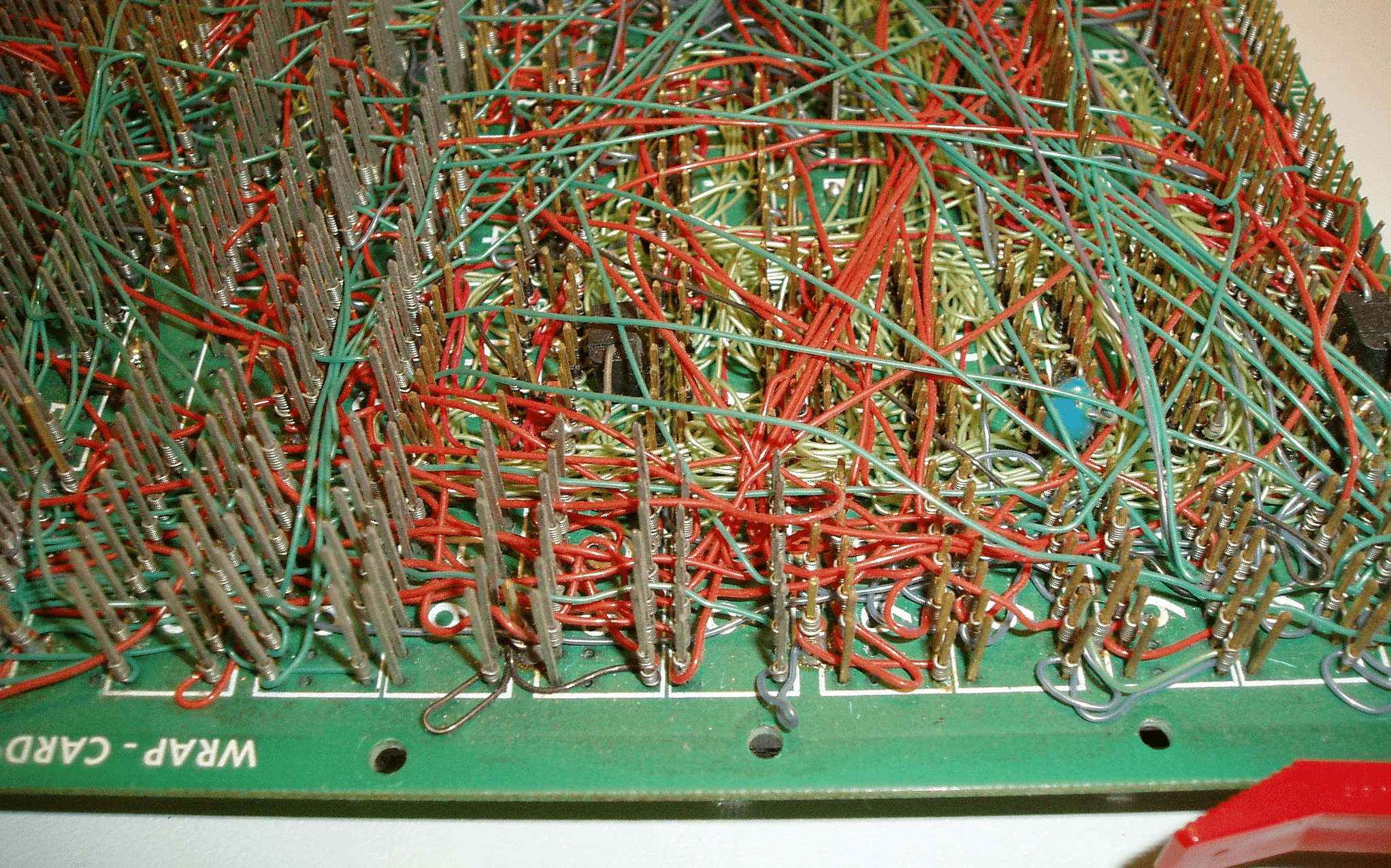
Manual Routing
PCB Routing
Well that’s not the case today thankfully because in 20th century too people understood that ‘size matters’, which led to 20th century’s one of the most important invention- Printed Circuit Board (PCB).
What is PCB?
Developed at the end of 1930s by an Austrian-born inventor, Paul Eisler, it is considered as an elixir for today’s mass production of radio, T.V, automobiles, semiconductor, electronic gadgets like phones, microwaves, laptops, you name it, but even in 2022 Printed Circuit board is not easy manufacture. It requires various parts, machinery’s, tools and materials.
Composition
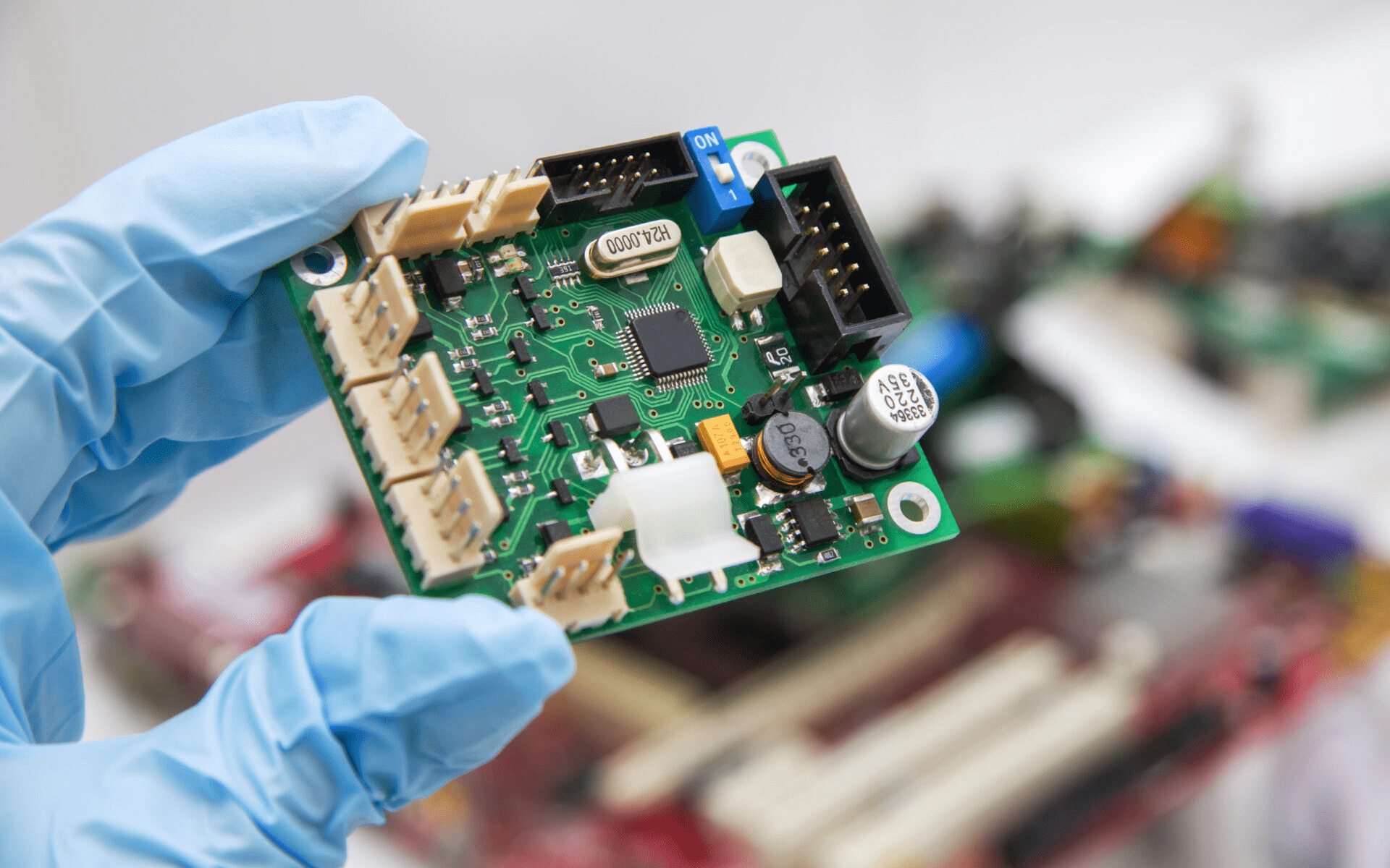
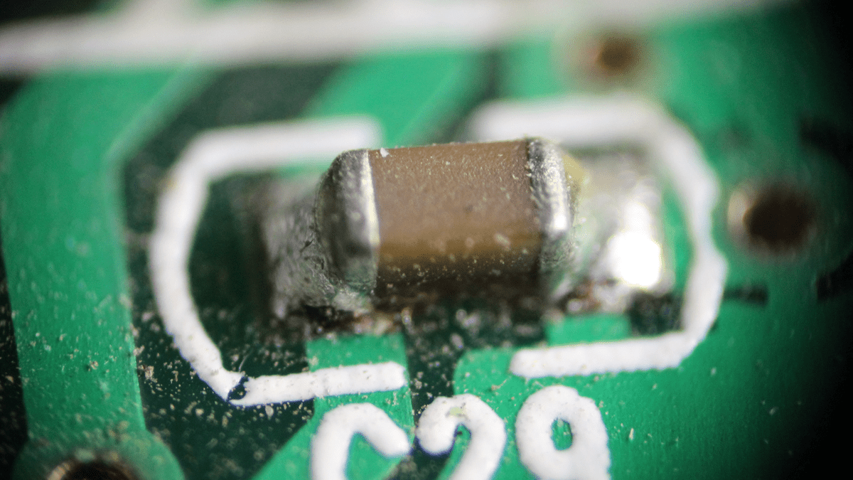
Printed Circuit board is a thin laminate sheet made up of fiberglass generally but also composite epoxy at times. It mechanically supports and electrically connects conducting material and electronic components.
PCB Composition
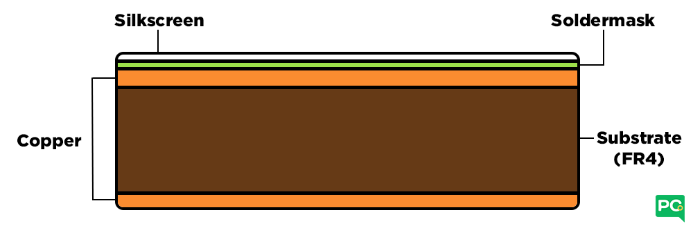
- Base – PCB is a thin laminate sheet made up of fibreglass (FR4) as its base material or substrate. This solid core gives the PCB its rigidity and thickness. It mechanically supports and electrically connects conducting material and electronic components. Cheaper PCBs and perf boards are made with other materials such as epoxies or phenolics which lack the durability of fibreglass but are much less expensive.
- Copper – Conducting material is mostly copper just like our traditional wires but a much miniature and embedded version of it running throughout the lengths and breaths of the PCB. It’s just like the veins in our body. The electronic components usually found sitting across the PCB are capacitors, resistors, translators and diodes. It’s just like the organs in our body. Copper layer is laminated to the board with heat and adhesive next to the base material. PCBs may have copper layer only on one side or both, further the number of copper layers can go on to 20 or more depending on the requirement.
Wondering why copper?
Its due to its high electrical conductivity and easy availability at low cost in comparison to other high conducting materials like silver or gold.
- Solder mask – The layer on top of the copper foil is called the solder mask layer. It protects the PCB surface and insulates the copper circuit from oxidation from the environment, accidental contact with other metal, solder or conductive bits. It gives the green or other desired colour to the board, however solder mask is applied in such a way that it cover up the small traces but leaves the silver rings and SMD (Surface Mount Device) pads exposed so they can be soldered to. It also makes the PCB high temperature resistant. A solder mask is nothing but a layer of polymer.
- Silkscreen – On top of solder mask, a white layer of silkscreen is applied. It is used for nomenclature on the board by adding letters, symbols and numbers to the PCB that makes assembly and working convenient.
- Mounting – Once the layers are stacked just like a lasagne, various mountings are made on the board, so it can interact with different board or with different component within the board.
- Annular rings – gold/nickel plated around the holes on the board.
- Finger – exposed metal pads along the edge of the board, used to create a connection between two circuit boards.
- Via – a hole in a board used to pass signal from one board to another.
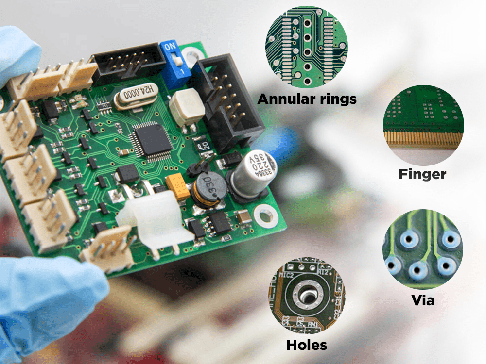
Mounting Options
- Electronic Components – Few of the electronic components generally used are as follows:
- SMD / SMT – (Surface Mount Device / Surface Mount Technology) These are tiny components which are placed on one side of the PCB and does not affect the components on the other side. Smaller footprint and easy to mount on PCB using robots and machines.
- THT – (Through Hole Technology) These are components with long leads which passes from one side of the PCB to other side, which can be advantages or disadvantages depending on the design. But takes larger footprint and difficult to mount these components on PCB using machines and robots.
SMT– Surface Mount Technology
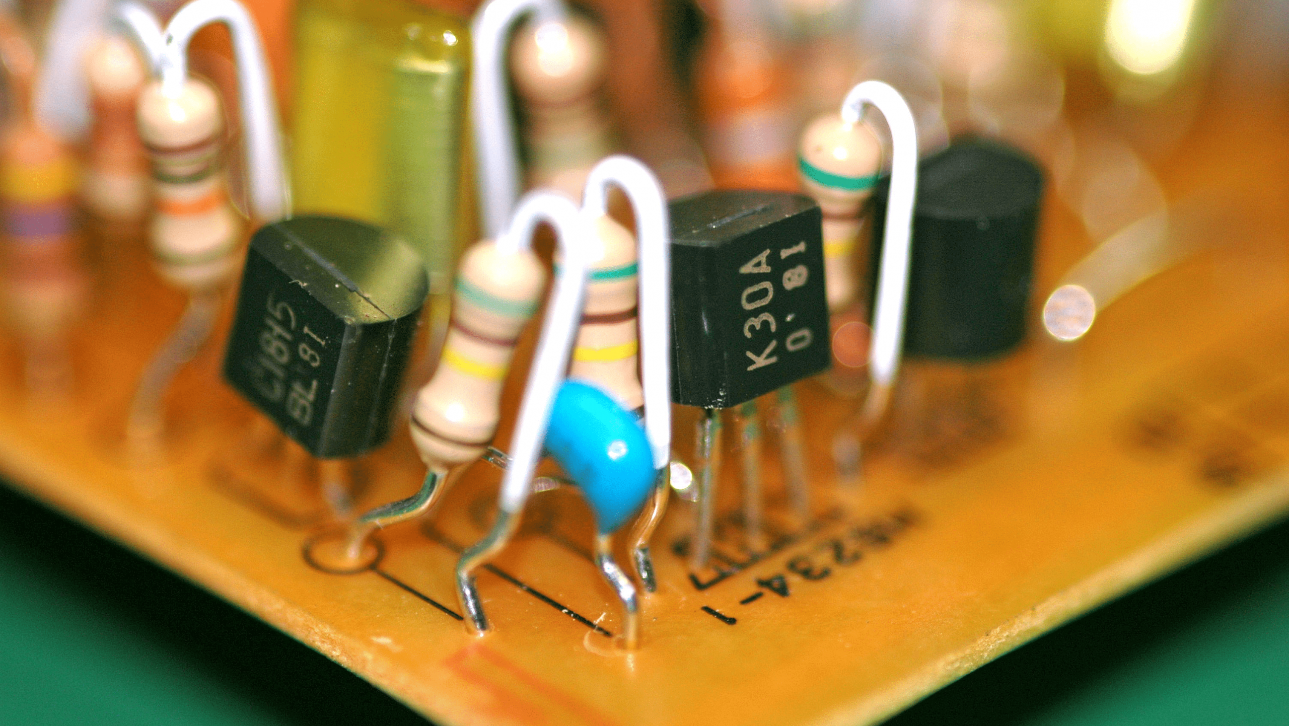
THT – Through Hole Technology
Hope the composition and their functions are clear by now. The key point here to understand that Printed Circuit Board(PCB) is just the structural layout of a PCB and may or may not have components soldered on to it. While PCB or printed circuit board alone means just the blank board with copper tracks. Whereas PCBA (Printed Circuit Board Assembly) is the process which will make the complete sheet with all its materials and electronic components with ready to perform desired function which allows carrying of signals from one part of the device to other.
Types of PCB
Since PCB is just a structural layout, manufacturers also manufacture this in various types depending on the application.
- Single-Sided PCBs
- Double-Sided PCBs
- Multilayer PCBs
- Rigid PCBs
- Flex PCBs
- Rigid-Flex PCBs
PCBs range from single layer to multi-layer arrangements. Former being used in simple devices like our T.V. remotes while latter used in smart watches, supercomputers in much complex arrangements.
“The number of layers is referred to as the number of separate conductor patterns – usually even and including the two outer layers. Most boards have between 4 and 8 layers, but PCBs with almost 100 layers can be made”
— QualiEco Circuits Ltd
Further, it can be classified based on flexibility ranging from rigid, flexible and rigid-flex. However, Rigid PCBs are widely used and easily available at affordable costs it’s the most of people think of when they hear the word PCB.
Why are PCBs Important?
The cost effectiveness of PCBs makes them ideal for supply chain demands and cutting production cost of the products. Its utility covers wide horizon, ranging from-
- Industrial and Commerce– the consumption based economy that is driven by ITC needs everything quick, efficient and a click away. Such electronic control of our mechanical and electrical devices is only possible with the PCB used to serve ranging functions of making internet surf using network data on phones, laptops or tracking steps on smart watch or baking cake on touch panel based microwave oven or driving the car or using solar energy using PV cells.
- Medical– PCBs are used both as rigid frame in medical imaging devices, MRI machine or flexible frame in pacemakers or microchips used from internal examination of the body.
- Aerospace and satellites– in flight communication, drones, etcetera. Here the quality of electronics and PCB is put to true test as this is one of the worst case scenario to use the PCB.
- Military– for making modern weapons, smart fencing at the borders of the countries, surveillance, all of these lined for defending the country, runs with PCBs in its core.
PCBs are Glamour
With increasing centrality of PCB in almost every device used today by the people, the demand rise of PCB is causing increased interest of manufacturers, producers and investors to bid on them. Thus, with globalised supply chain functioning, PCB manufacturing and designing today opens a window for exploring entrepreneurial fortune for today’s enthusiasts.
Amid Covid hangover, the global PCB market is expected to reach $72.7 billion by 2026 as per Global Industry Analysts Inc. (GIA).

Market capital by 2026
So yeah, PCBs are glamour for electronic industries in particular and global economy in general. Soon, we’ll be talking about those processes in detail in coming articles along with sharing experiences of manufacturing expertise coming from experts, will help understand the design and manufacturing of PCBs better.

Leave a comment