
Once you have finished the design and manufacturing. The final step before testing is the PCBA (Printed Circuit Board Assembly) process.
Overview
In PCB manufacturing, while the first step was to prepare the board that serves as the platform, the second step PCBA is placement of the components on that platform.
Today PCBA is done mostly automatically using varies industries automation techniques. However, in a DIY PCBA it involves mechanical work, precision and manufacturing which is the most fun part of Do It Yourself. However, before you start PCBA, an important decision that you made during PCB design i.e. choosing between through hole technique (THT) and surface mount devices (SMD) will decide the kind of assembly procedure you’ll follow. If you are just getting started we highly recommend choosing the THT method.
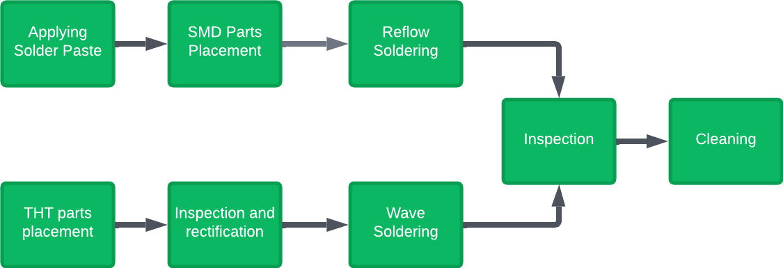
Process to completely Assemble a Printed Circuit Board
Overview Step-by-step procedure for PCBA
Step 1: Going through the BOM (Check for missing parts / Virtual components)
Step 2: Coating solder paste using stencils (Mostly done for SMD)
Step 3: Pick and place for SMD / THT components
Step 4: Reflow soldering for SMD/ Manual soldering or Wave Soldering for THT
Step 5: Inspection and cleaning
Going Through BOM
The Bill of Materials (BoM) is a comprehensive list of parts that includes reference designators, component value, Component package, quantity, and Manufacturer Part Number (MPN). Most of the BOM can be generated internally within the design CAD which outputs spreadsheet file or .CSV file. All the Assembly house require a well defined BOM, clearing giving all instruction that is required just like the table below. But sometimes this also can vary from one Assembly house to another. If you are more interested in automated assembly, Circuitstate have an excellent article on how you can prepare your board design for fully automated assembly.
| SL. No. | Reference | Value | Description | Package | Quantity | MPN | Notes |
| Sequence Number | Designator | Value | Specs | SMD/THT Packages | Required Quantity | Manufacturer Part Number | Extra Notes |
If you have manufactured a PCB using KiCad for prototyping you can use ibom. Which is a open source plugin to make a interactive BOM, which can be used during assembly process with any browser. This ibom can help in tracking of components placement, tracking sourced components and filtering unplaced components, etc.
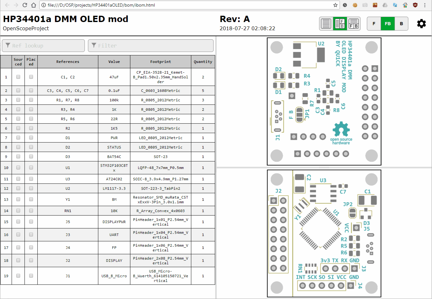
IBOM – Picture Credit Hackaday
Applying Solder Paste Using Stencils
[This steps is required only if you have SMD Components]
What is Solder Paste?
Solder paste is a mixture of minute solder spheres held within a specialized form of solder flux. As the name indicates it has the texture of a paste, and hence the name. Traditionally this used to be tin and lead, but with the legislation has been introduced around the world, to only use lead free solders. These may be made from a variety of mixtures. Some of the mixture components are 99.7% tin and 0.3% copper or 3% silver, 0.5% copper and 96.5% tin whereas there are other mixtures that include other metals including tin.
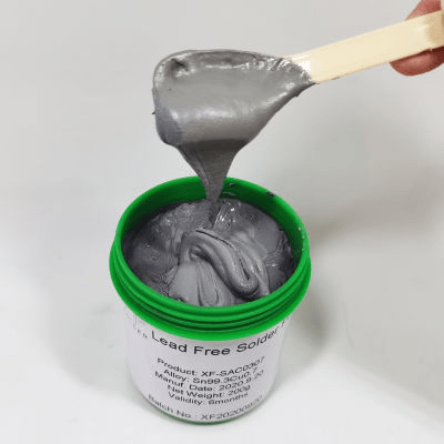
Solder paste
The solder paste stencil is the sheet of metal like stainless steel or nickel that has holes cut very accurately according to the solder paste layer of PCB layout design. The stencil and PCB board are attached together to align them firmly and the solder paste is spread over the stencil using a squeegee. This way the solder paste is put only at desired locations on the PCB.
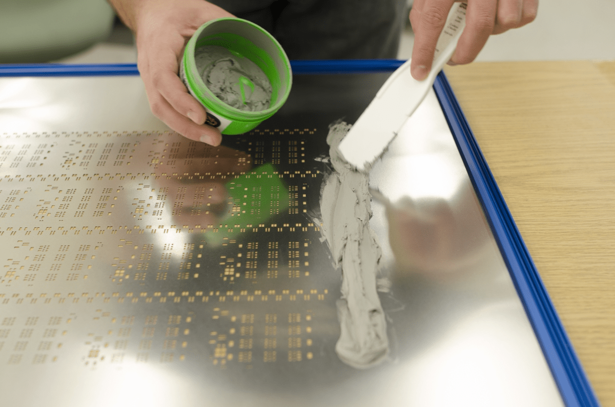
Applying Solder Paste – Image Credit: Sparkfun
Also, if you couldn’t manufacture the stencil, you can also directly put the solder paste using a smaller spatula or by using solder paste dispenser syringe.
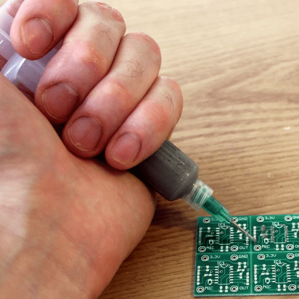
Solder Paste Dispenser
Part Placement : SMD / THT
Note : Always start with placing the smaller components so it won’t be affected later when a larger component is placed and obstructing the smaller footprints.
Once the paste is applied on the PCB board, place the required electronic component on top. This can be done by hand or by a machine. Using tweezers is a great way to place SMD components. But to make proper solder joint later, ensure to place the pins of the components in the centre of the applied paste.
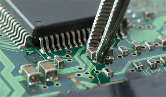
Align the components and the pins
In case of a large factory, a conveyor belt often carries the board directly from an paste deposition machine into the pick-and-place machines to place all the SMD parts. One of the advantages of using SMD technique is that very small components can easily be placed on the PCB board easily by a pick and place machine, while this process may be difficult in case of THT components.
If you opted for THT components during the design of the PCB, there is no need for a surface preparatory step of applying solder paste as done for SMD. Directly place the electronic components on board by inserting the components in designated holes. This process also can be automated but it would be more expensive and complicated for the THT components but this is the easiest method for someone getting started with printed circuit board and soldering.
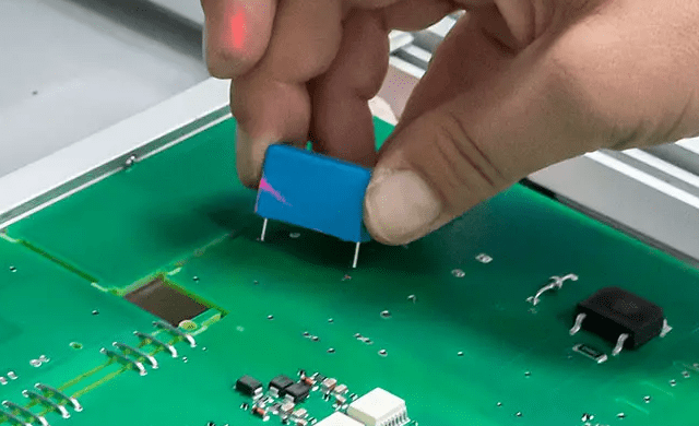
THT Components Placement
Reflow Soldering for SMD/ Manual Soldering for THT
For SMD: Reflow
After pick-and-place, to create a solid solder joint, the solder paste is reflowed. The boards are put on a conveyor belt that moves slowly through a large oven, exposing the boards to enough heat to melt the solder.
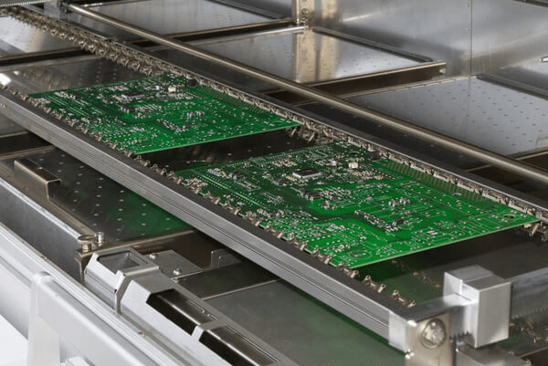
Hot Conveyor Belt System
However, for DIY PCBA one can simply use a reflow gun or use a smaller heat bed.
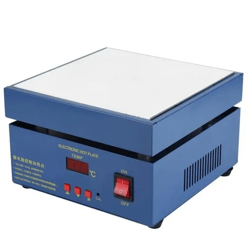
Hot Solder Plate
For THT: Manual Soldering
In a larger production facility, the soldering of through-hole components may be done using a technique known as wave soldering, where the board is passed over a standing wave of molten solder, which adheres to component leads and any exposed metal on the board.
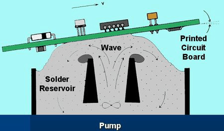
Wave soldering
However, at home a usual soldering iron can be used to solder the components on the board. For this, an ironing rod of 15-30 watt can be used. Make sure you align it at 45 degrees while using and leave no leads unsoldered or partially soldered. For a proper soldering technique, solder is heated beyond melting point, so make sure you use enough solder that adheres to the board.
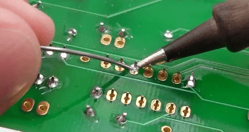
Manual Soldering
Inspection and cleaning
Once the component placement is done, clean the board and the components with solder wick for excess solder spill and isopropanol to clear off any spillover of excess solder flux or dirt.
Also inspect if all the components are soldered properly and non of them are misaligned or miss placed. In industries they follow certain set of testing procedure to ensure if the PCB is assembled properly. You can read about it here.
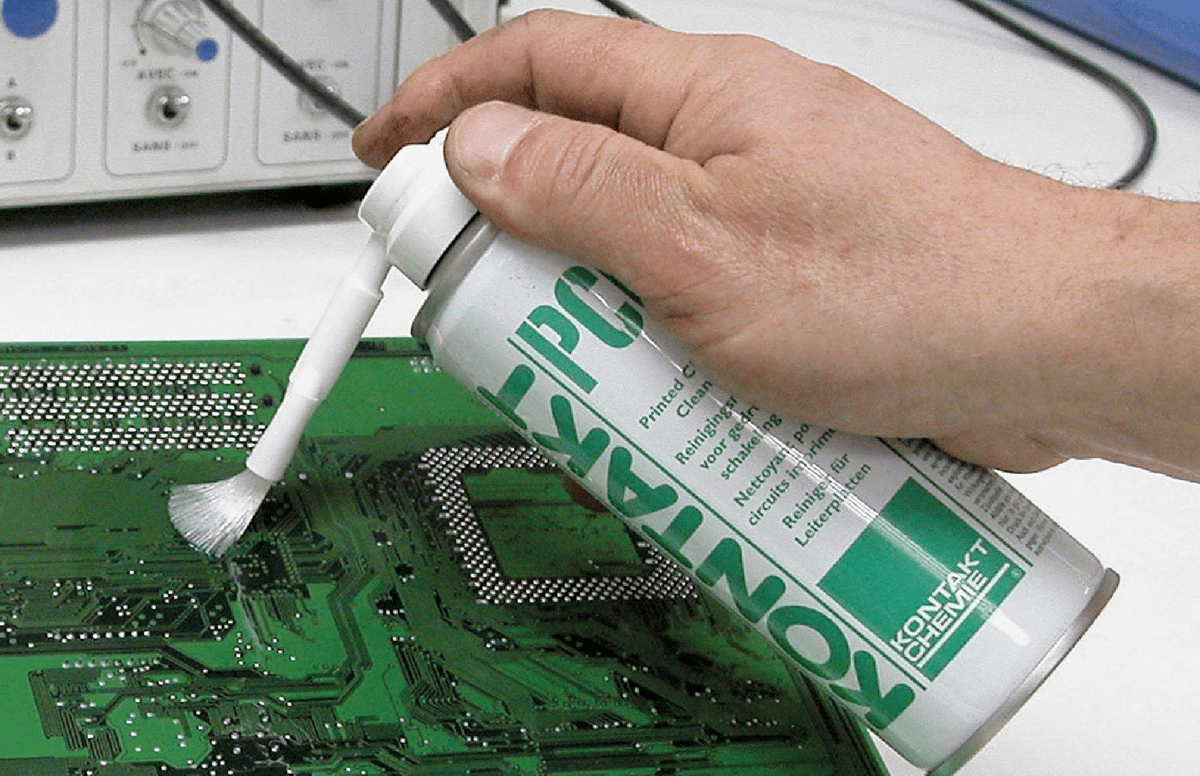
cleaning using isopropanol
This completes your assembly process and you can use your PCB as per desired work after PCB testing.
If you are a beginner it is advisable to go for through-hole technique for soldering the devices since it’s comparatively easier and requires less tools which are easily available. Surface mound is mostly preferred by those who are working with very small devices and producing PCBs at huge quantities.
We hope this step-by-step guide to assembly will help you throughout your PCB assembly journey. Any query at any step, you can simply post it on the QnA section and the whole community would be happy to help you!

Leave a comment