PCB Testing is as important as the exam for doctors, even if it’s COVID you can’t skip it. When we say test, it might remind us of some rough days but ignorance in PCB testing now can surely bring more rough days ahead.
Necessity of PCB Testing
Nobody wants a Printed Circuit Board (PCB) that falls short on performance in real-life working or suffers from sudden death or has a shorter lifespan due to defeats that were ignored during manufacturing.
Testing help in :
- Identify critical errors early on
- Increase yield and reduce costs
- Improve overall quality and safety.
- Better understanding of what works and what doesn’t
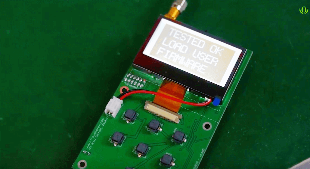
Image Credit: Seeed Studio
Different PCB Testing Methods :
There are multiple PCB testing technique can be used to get the long lasting and perfect working device.
To make it simple for you, we are breaking it down into pieces by classifying the various tests into three main heads.
- Mechanical Testing
- Visual Testing
- Electrical Testing
Within each type, there are various subtypes which are part of manufacturers’ arsenal. We will understand them one by one.
Mechanical PCB Testing
These tests are mainly conducted during the manufacturing stage of the PCB and often this is not something the designer would bother. Usually this type of testing is done by the manufacturers even before they start receiving orders from clients. From the results they obtain, manufacturers set the standards and the limitation of there production.
Various types of mechanical testing are:
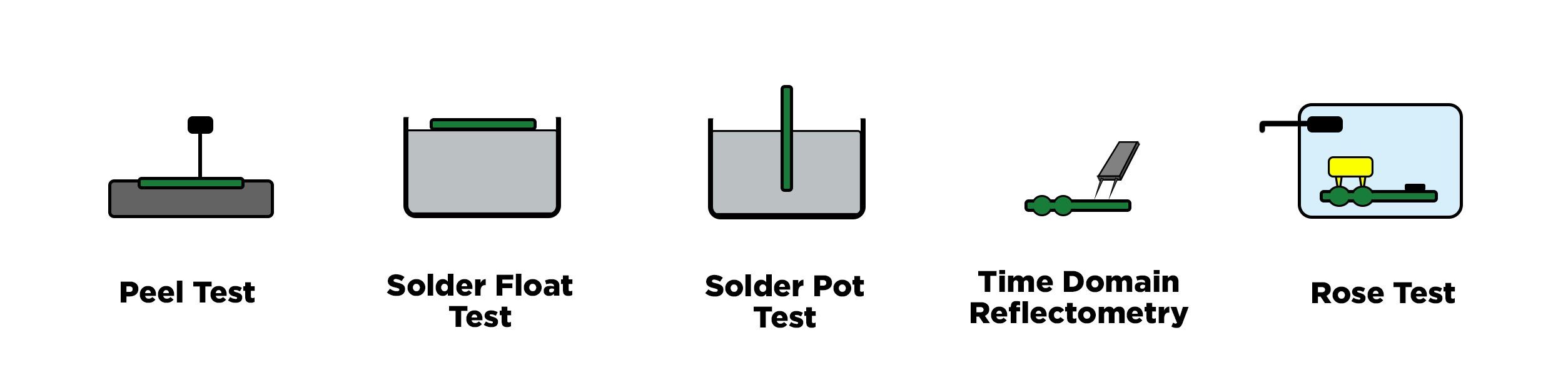
various mechanical testing
- Peel Test- The measure of strength required to peel the laminate from the board, thus checking the adhesion between the conducting layer and the dialectic core material.
- Solder Pot and Float Tests- Determines the solderability of plated through holes and the level of thermal stress a PCB’s holes can resist.
- Micro-Sectioning Analysis- Investigates defects, opens, shorts, and other failures.
- Time Domain Reflectivity- Used for high-frequency boards.
Visual Testing
Visual inspections are used both at level and industrial level. This is one of the safest test to perform on a PCB without damaging it or applying any stress on the components or the physical structure.
Various types of Visual Inspection:
- Manual Inspection
- Automated Inspection
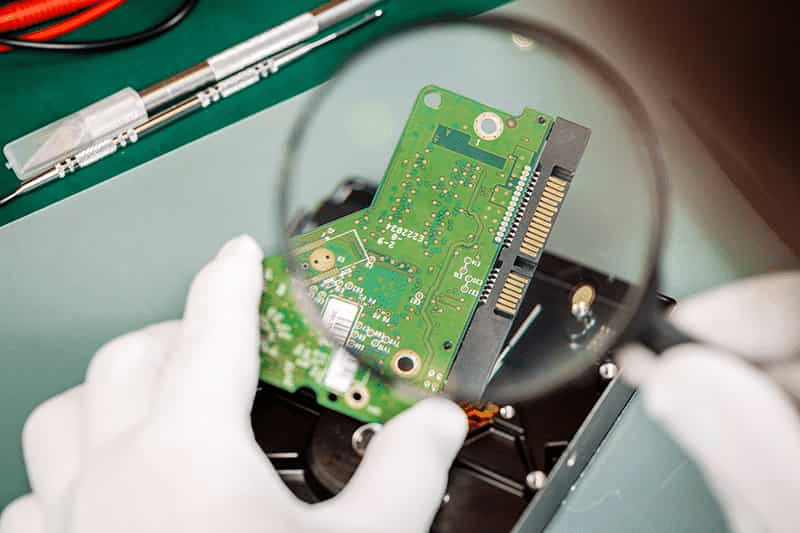
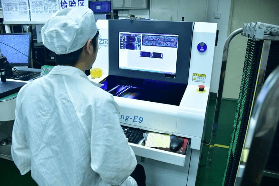
Manual Inspection
In manual inspection, a magnifier or sometimes the technician’s bare eyes are used to manually find solder defects and other visible defects such as component orientation, missing components and board stains. This is the simplest and most basic inspection method. This is what mostly followed when the prototype is done in very low quantity.
visual inspection
It’s cheap and easy to set-up – no test fixture or lengthy set-up required. Most major solder defects can be identified by it. However, this can be subjected to human errors as it depends on the technician’s skill. Also, one of the major disadvantages is, it can only inspect visible solder joints, thus hidden joints and underside joints which can often happen in SMD (Surface Mount Device) cannot be evaluated.
Therefore, it is ideal for simple designs with fewer components and lower quantities. This would be the ideal case if you are just getting started with PCB design and manufacturing.
Automated Inspection
- Automated Optical Inspection (AOI)- It is used in industries where PCB manufacturing takes place and are placed in the production line itself and provide first hand quality assurance. AOI uses a single (2D) or two (3D) cameras to take high-resolution images of the PCB, and compares these with images with a template board or with a database of images of good and bad boards. AOI covers all the checks manual visual inspection would identify with greater accuracy and consistency and can identify incorrectly placed components thus they are more accurate than manual visual inspection. Though most major solder defects can be identified, AOI is a passive testing method and can only detect surface defects.
Automated Optical Inspection
- Automated X-Ray Inspection (AXI)- It uses X-rays that can penetrate the PCB and body of components to generate 2D or 3D images of the solder joints. This makes it ideal for hidden joints such as those on Ball Grid Arrays (BGA) and flat no-leads packages. AXI inspection can also detect solder voids and many other optical inspection methods cannot.
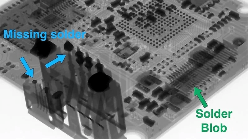
X-ray inspection
Among the three visual tests (Manual, AOI, AXI), Automated X-Ray Inspection is the most accurate and has the highest defect detection rate. However, it requires proper set up which is ridiculously expensive, might required multiple certification from different organization as it deals with X-Ray and majorly needs skilled technicians to operate it.
Visual inspections seems very promising but they alone are not enough for commercial PCB testing and are clubbed with various electrical testing methods to get most reliable results.
Electrical Testing
While mechanical testing is ideal during the manufacturing stage and visual inspection is mostly passive testing which identifies flaws only at tangible levels, electrical testing is the active testing method that tests the PCB in a prototype working environment to identify functional flaws and passes.
There are many electrical PCB testing methods; here we will discuss the top PCB testing methods which are commonly used:
- In-Circuit Testing (ICT)
- Flying Probe Testing
- Burn- In Testing
- Functional Testing
In-Circuit PCB Testing Method
In-circuit testing systems are found typically on every PCB manufacturing line in industries and its fault coverage range between 90% to 95%.
It captures manufacturing defects so that rework at functional test is reduced. Common defects that are detected by it are: Tombstonning, Solder shots, Missing, lifted pin and Poor soldering.
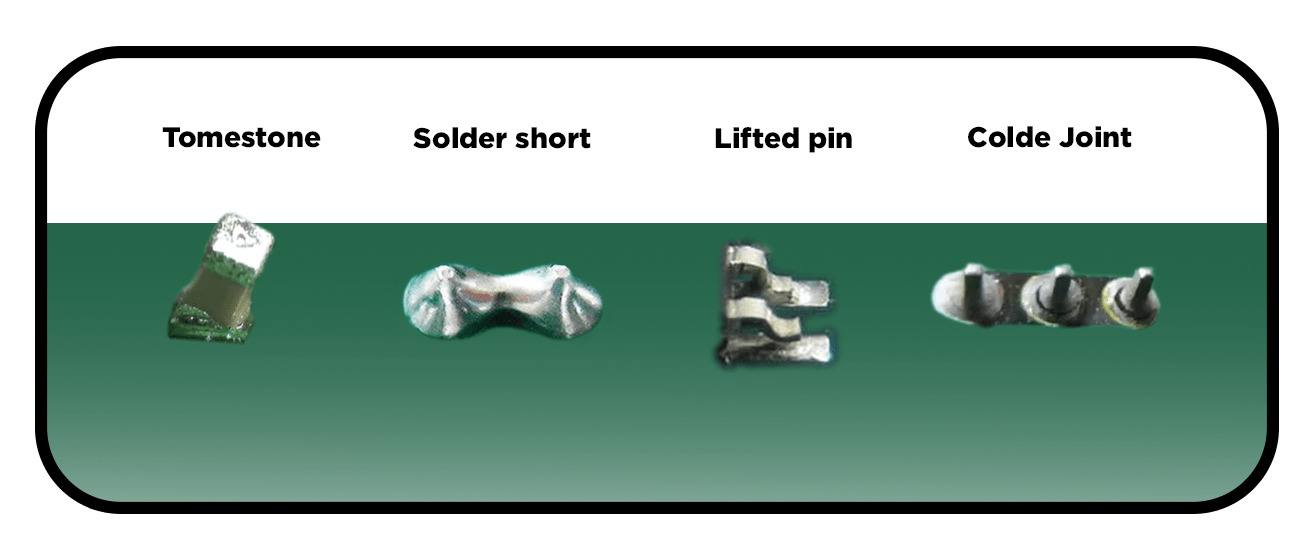
Solder Defects
This type of test can get very expensive depending on the number of components on the board and the complexity of the board. In this stage the board powers up and actuates the individual circuitry to get accurate results. It is also known as a bed-of-nails test.
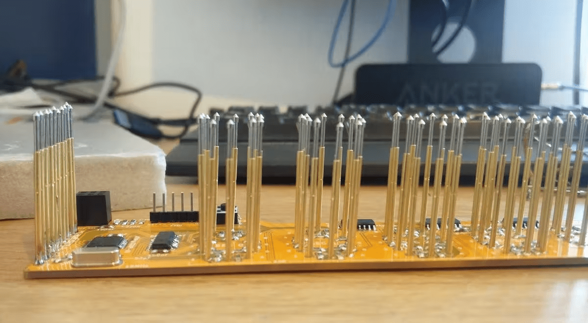
Bed of nails
This test involves using fixed probes laid out in a way that matches the design of the PCB which the designer have to place testing point for jigs. Because of which every PCB needs a custom test jig contains boards, fixtures, various testing circuit and hooked up to a external monitor or a simple indication system which will display the result as pass or fail. The bed of nails tester simply pushes the board down on the bed of probes to start the test and put certain amount of pressure on the connection to make sure it stays intact. When the probe come in contact with the testing pads on the PCB, the ICT testing circuits makes a connections with the PCB circuit to test various characters of the PCB (data transmission, voltage drop, current consumption, etc).
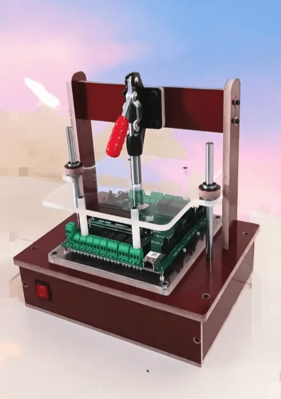
Test Jig
It is used for mature product with thousands on production mostly because of the time for making the jig and high set-up cost involved.
Flying Probe Testing
The FPT process uses needles attached to a probe on an x-y grid obtained from basic CAD. It is a non-powered type of test that directly checks diodes, transistors, passive parts, performs voltage measurements and also it can access non-tented vias which weren’t accessible by ICT method.
One of the advantages of FPT over ICT methods is that it’s less expensive (for designers) as there is no need for a sophisticated fixture. But it does come with a higher cost for the manufacturer as the this system can cost 10X more than the ICT testing. But this can be programmed to run test on different PCB without having to invest in a new test jig.
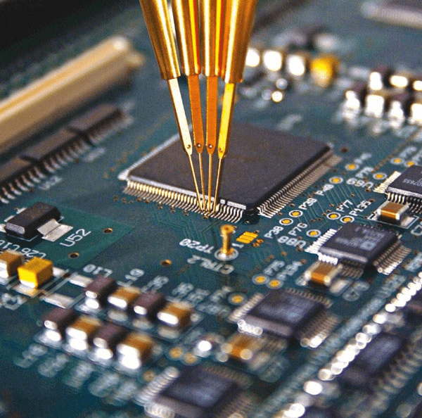
Fly probe testing
Burn-In Testing
During burn-in testing, boards are subjected to conditions (such as power supplied, voltage, current and temperature) exceeding the rated operating conditions and over a longer period of time to detect early failures and test load capacity, thereby eliminating premature failures in the field. Unlike other methods, the burn-in testing method triggers failure to prevent catastrophe in a later functioning stage.
It helps the manufacturer identify the cause of defect and thus rectify the original design to accommodate necessary changes.

Burn-in testing
Functional Testing
This testing method powers the board and checks the functional ability of the device under test as intended. It stimulates operating environment conditions for the board. One can check a few devices on board or put the whole board to test, this mainly depends on the complexity of your board design.
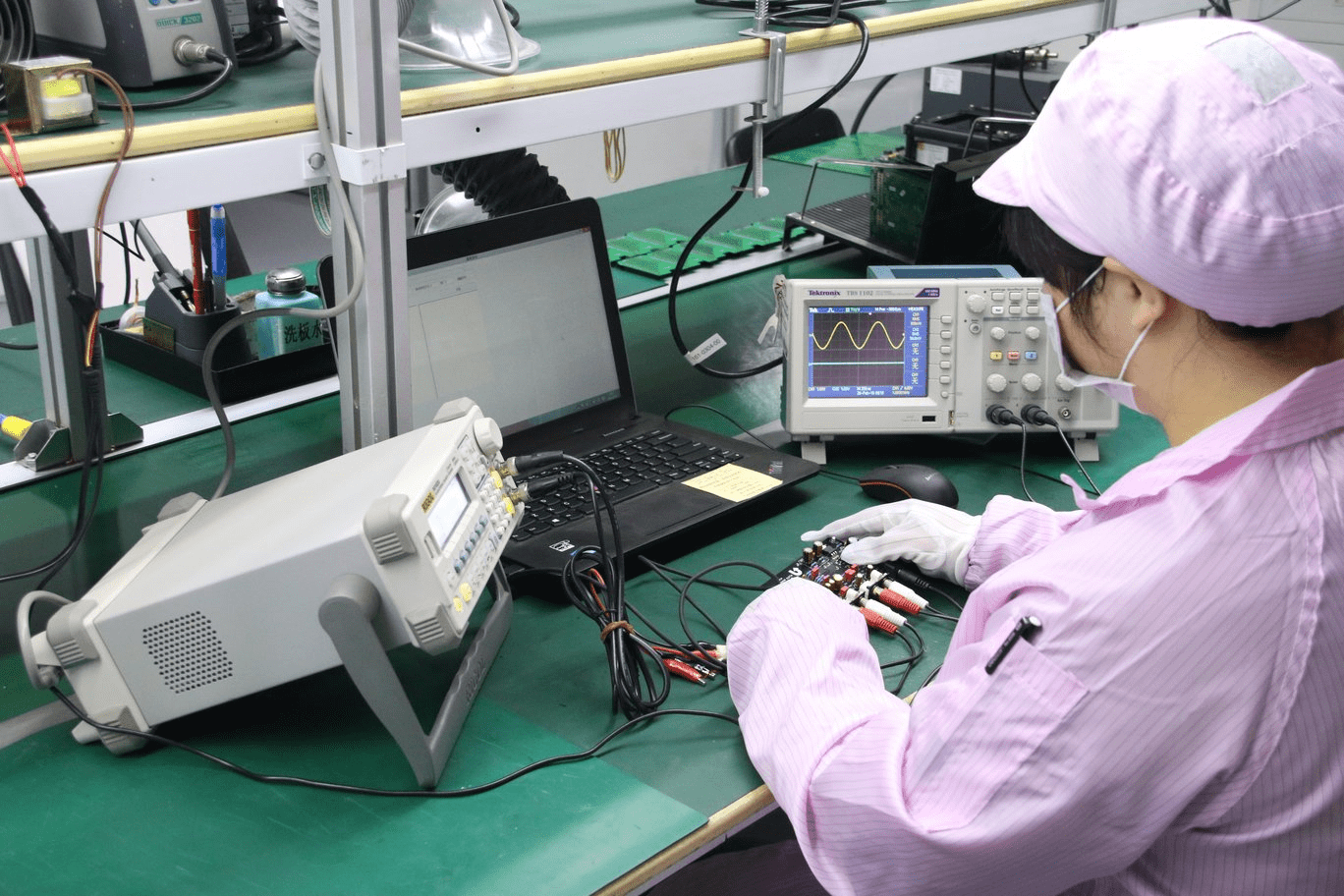
Functional Testing
Due to its flexibility and minimal cost involved, it is widely used by DIY PCB designers, solo or small-batch manufacturers. However, unlike burn-in testing, functional testing cannot check the cause of early defect of component failure or shorter lifespan of PCB.
Conclusion
PCB testing methods range over a spectrum and are widely classified, thus giving its designers a choice pool to pick from. Every method has their pros and cons as discussed. Depending on the scale of manufacturer, level of testing needs, cost involved and use of the PCB, one can choose accordingly.
As a beginner too, one can thoroughly put their PCB boards to testing such as visual inspection and functional testing. Therefore, avoiding the whole hit or miss conjecture about their PCB. If you like to know more about Printed Circuit Boards you can read our Extended Basic.

Leave a comment