
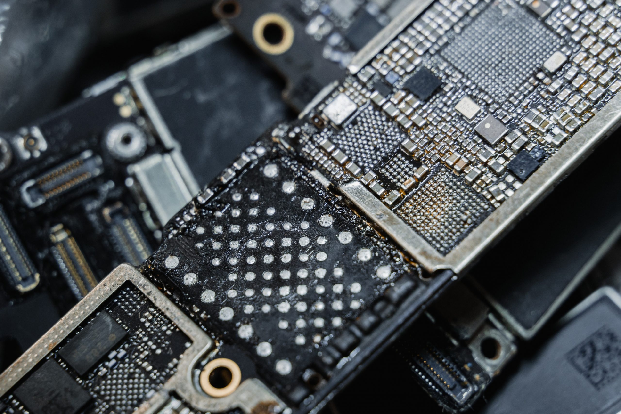
We all like tweaking around rules or breaking the rules or making our own rules, however messing with rules while designing Printed Circuit Boards could cost you a lot. Designing a board with passion, love, affection but its a heart break when it does not work as expected even though everything seems good. That’s because we miss the nuances that professionals use during their PCB design process. You can still fix the poorly designed board later but a minor tweak can cost you a fortune in manufacturing and production down time, so it’s better to get it right at the sooner than later.
So, we have put some fundamental guidelines that we suggest you not to overlook in PCB designing (Including beginners):
Making the Right Choice While Choosing the Board
The board is the foundation on which rests everything that sits on your PCB. Therefore, randomly choosing any board without clear vision of size, shape, strength and number of layers can prove detrimental while assembling.
Therefore, one needs to follow rules while choosing the board (board stack up):
- Adequate grid space for the circuit – This is to avoid either wastage of extra space on the board that wasn’t needed or congested frame due to over-loading of components. An over-loaded board can affect working on the board due to chaotic assembly and also impact signal flow. Therefore, a clear estimation of the grid size and adequate grid space for circuits should be a thumb rule.
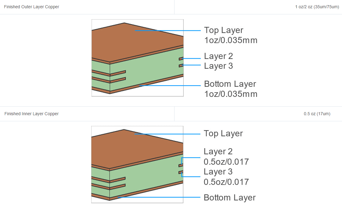
- Determine number of layers required – While a single layer is sufficient for simple design, complex designs may have many tracks, routing them will require multiple layers. Therefore, knowing the exact number of layers needed will help in making the process smooth and fast. It’s advised to check with multiple manufacturers, what would be the cost increment as the the number of layers increase. Overall by using lower layer count board, the PCB can be optimized for cost as well as design, assembly and testing time.
- Determine the board material – Always choosing the same material for your PCB isn’t the best choice. The board material can be decided based on various factors :
- Glass transition temperature – TG is the point at which a PCB loses its rigidity and its ability to perform well. So depending on the temperature your material with higher or lower TG.
- Copper thickness or weight of Copper – It’s the amount of copper that’s on the PCB. If your board have to distribute DC power across a large board there might be a voltage drop (usually in mV) and this in turn dissipate as heat on the PCB. In other hand choosing the board with lower copper weight will help in decreasing the cost of the PCB as well as decrease the waste produced.
- Other factors to consider – If you are designing a complicated board or high speed PCB you might also need to consider Decomposition Temperature (Td),Coefficient of Thermal Expansion (CTE),Thermal Conductivity (k),Dielectric Constant. It might be “OK” if you skip some of this selection for simple PCB, as most of the PCB manufacturers take care of it.
Selecting the right types of PCB for the intended purposes is important in achieving the best possible Function, Longevity and Cost efficiency.
Grouping of Components (Separating Analog and Digital)
The designer should read the schematic and breakdown into sub-sections depending on the circuit function. For instance: Analog, digital, high-speed, high-current, power supply, etc.

- To begin with, avoid placing sensitive high-speed devices close to the edge of the board. This is because the edge of the board possesses different impedance characteristics and there is a higher chance of electromagnetic interference(EMI).
- The functional blocks of circuitry like power conditioning, RF, digital, Analog, etc., should be arranged as groups to reduce signal crossing.

- Apart from the circuit function, the voltage and current levels should be analysed. Circuits with similar VCC and GND should be grouped and placed together.
- Avoid placing components of a different functional group in the midst of another circuit. For example, separate Analog circuits from digital circuits. When Analog and digital currents overlap each other, this degrades the Analog signals due to crosstalk. However, when Digital and Analog are isolated, the digital return current does not interfere with the Analog.
PCB Floor Planning (Component Placement)
A floor plan is rough sketch that allocates general areas where components are to be placed on the board. Components on your PCB are just like organs connected through veins and arteries in our body. Thus, carelessness in their placement can affect the functioning of the whole PCB.
A pre- planned component placement will allow the designer to optimize the circuit for signal integrity. The below specifics will help in easy understanding of components placement.
- Load the PCB with the most vital components first – There are components which require specific location on the board or are vital due to their sheer size. It’s always advisable to first place such components on the board and lock-in their position to prevent complications later. For instance, choosing a location for transformers and power input terminals.
- Load the processors and ICs – Integrated Circuits and processors generally need to make connections with multiple components. Locating these components centrally makes the trace routing easier and stretching along the perimeters of the board giving it a neat and systematic look.

- SMD should be placed on one side – The Surface Mounting Devices should be mounted on the same side of the board. This will help in assembly as each side of the board will require its own pass down the SMD soldering line and doubling the production type, so placing on one side will reduce time consumption and assembly cost.
- Consider Routing channel – The wiring length should be optimized to prevent crossing over and voltage drop. This affects the latency and power in case of complex designs. You also have to consider the routing channels while planning the component placement to ensure there is adequate space.
Space for routing
NOTE– For components that need direct connections to power, it’s recommended to use common rails for each supply if a power plane is not used.
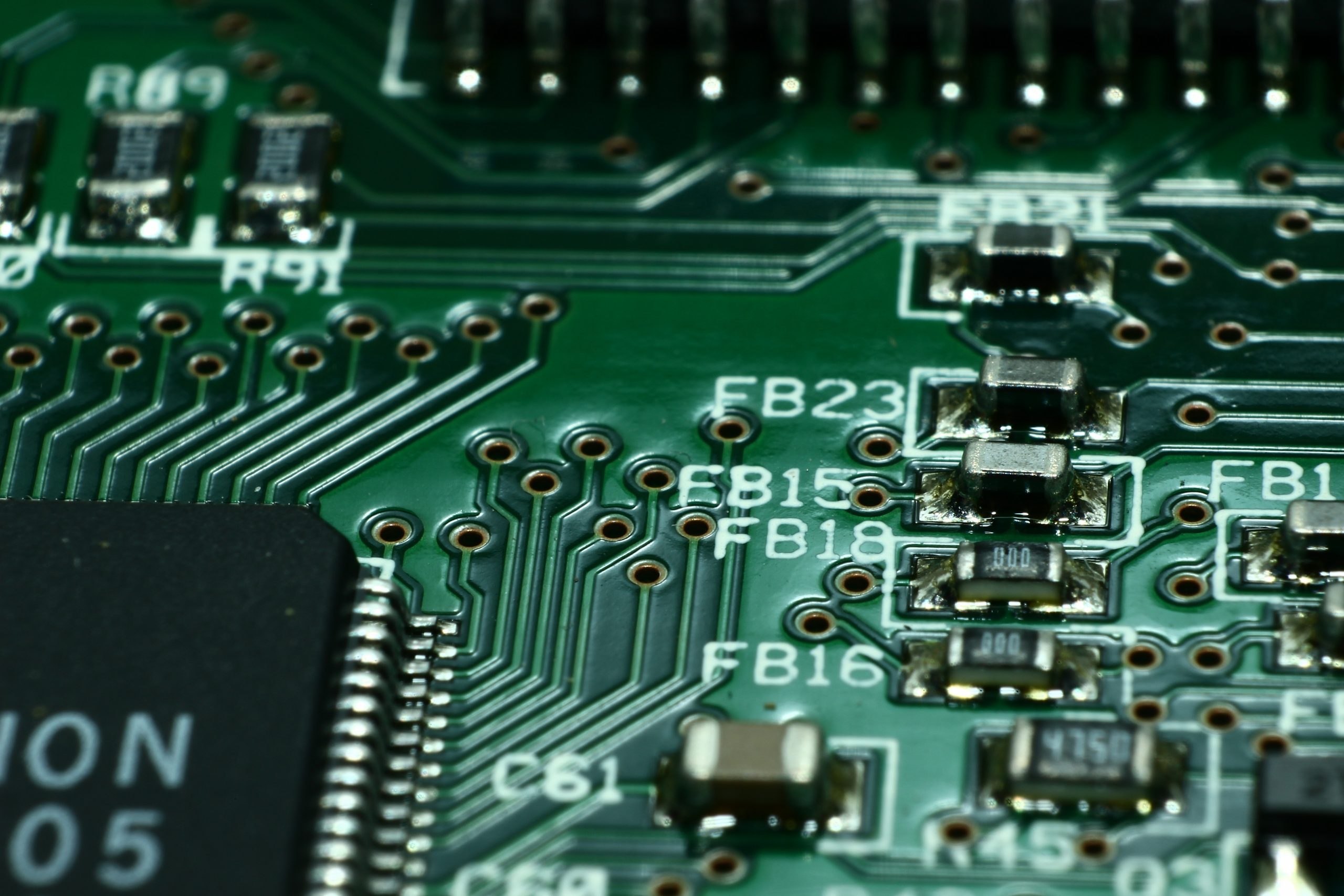
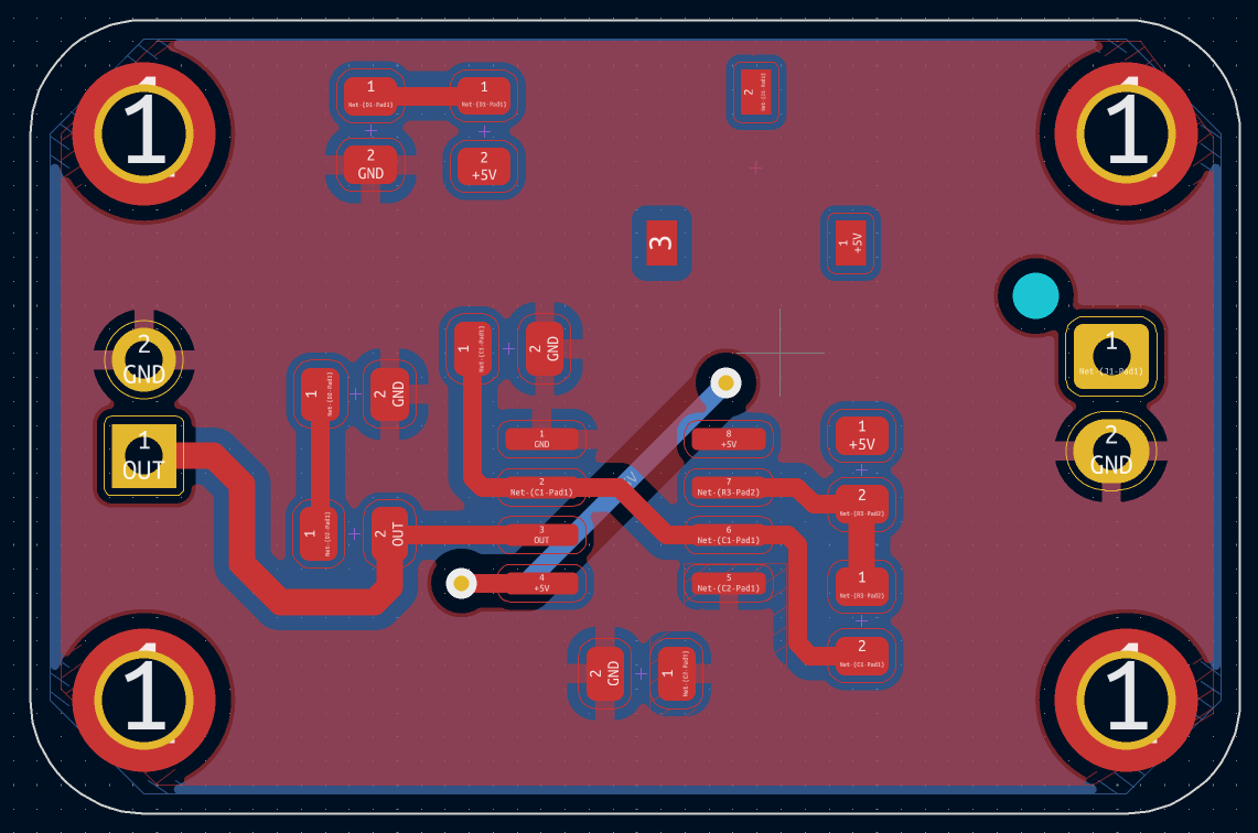
Follow Routing Guidelines
All PCBs need to have copper that connects components on the surface layer or internal layers, known as traces and the process of making this traces between the components is called routing. What qualifies as a “simple” device depends on several factors, which will determine the appropriate trace design you use in your PCB.
Thus, after arranging components on the board, it’s time to start connecting components with traces.
- Understand Your Manufacturer’s Specifications – Even if the design software allows you to do the traces very small to make the traces travel between the components, the manufacturer might not be able to manufacture it. So check with the manufacture before selecting the appropriate track width for your board design.
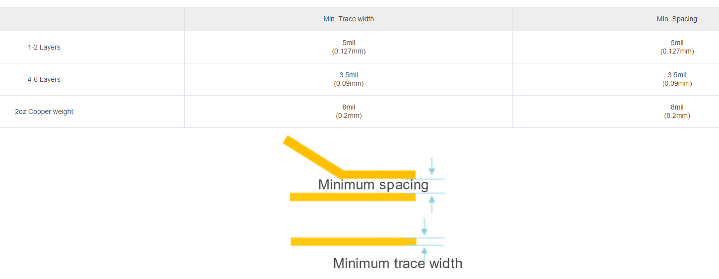
JLCPCB capabilities Detail
- Leave Enough Space Between Traces – PCB manufacturing process isn’t 100% precise and does come with some limitations so If you pack things too close together, then you’ll run the risk of a short circuit developing when your board gets manufactured and traces unintentionally connect.
- Make Your Power and Ground Traces Wider – Both power and ground traces will have more current flowing through them, and if you don’t make them wider than the signal trace, the power/ground trace will heat up trying to flow through narrow spaces, which can end up ruining the board on long run.

- Horizontal/Vertical tracing – Horizontal trace routing on one side of the board, then always route traces vertically on the opposite side. This is one of many important 2 layer PCB board design rules.
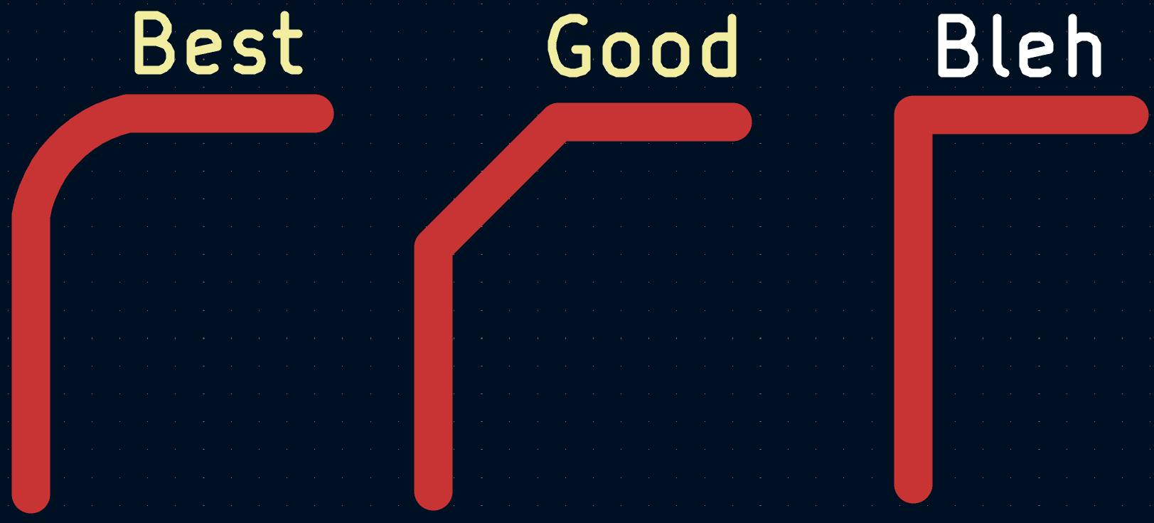
- Degree Trace Angles – This would be the god of routing guideline, ever engineer talk about if it’s beginner or professional nobody like seeing a 90-degree trace on there board. When you have a lot of traces have right angle turn, the outside corner of that 90-degree angle has the likelihood of being etched narrower than standard trace width. At its worst, this might get a bunch of 90-degree traces that aren’t fully etched, resulting in shorts.
This maybe little too much to remember while getting started, but with a few practice rounds and experience the routing will become easy.
Don’t trust Auto router! not just because it’s inaccurate, most importantly you’re the master of your own design.
How to Place Power and Ground Planes
As the components have been placed, to make them function it’s time to load the power and also provide a ground plane on the PCB board. For this, few considerations should be taken into account:-
- Ground planes are also often connected to components that get hot in order to help dissipate the heat.
- Using a ground plane between two active signal layers, the crosstalk between the signals on those layers can be eliminated.
- For any board board stack up, you should use ground planes instead of trying to route ground traces.
- Always implement continuous power planes unless there is a scenario where the design demands a split power plane. When dealing with split power planes, be cautious while placing the connected components across the split. The high-speed transmission lines should not cross the splits in power planes since it will break up the return path for those signals.
Focus should be on access to power and ground, as well as ensuring all traces have strong return path coupling to the nearest ground plane.
Design Rules Checks as much as possible
To help with the quality control process, it’s always recommended to start with Electrical Rules Check (ERC) and Design Rules Check (DRC) to verify that your PCB meets all established constraints. Electrical Rules check will help in any error made by the designer like short circuit, missing connection, etc. Design Rule check helps in defining gap widths, trace widths, common manufacturing requirements, high-speed electrical requirements, and other physical requirements for your particular application.
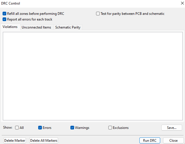
Design Rule check Interface – KiCAD
Although, running a design rule check at the end of the board design phase before preparing for manufacturing is normally suggested, one can run checks throughout the design process. This helps in identifying design potential problems early and corrects them quickly.
When the final ERC and DRC have produced error-free results, it’s then recommended to check the routing of every signal and confirm that you haven’t missed anything by running through your schematic one wire at a time.
Verify them before submitting for production
Various parameters have to be considered while manufacturing which need to be stated beforehand. Some of them are:
- BOM Cleaning – Why look at the BOM again before production if the components were chosen appropriately at the start of the design phase? The issue is that the supply chain may move rapidly, and your preferred components may be out of stock by the time you begin manufacturing. Prices might often fluctuate, putting budget strain on large volume buys.
- Mechanicals – Check mechanical elements in the PCB layout for positioning and clearances to other conductors. Mechanical parts such as mounting holes and vias should be examined to ensure that the hole diameter, pad diameter, and drill depth are correct. Some more sophisticated mechanicals, such as guide keys or connections, should be 3D examined to guarantee minimal interference.
These seven PCB design rules will help you throughout designing your own PCB professional style. However, experience and further in-depth knowledge about PCB and its various components will help you in becoming a pro in PCB designing.
You can read more about how to design a printed circuit board here.


Leave a comment