I’d like to request a video on pcb edge connectors. It seems in the KiCad 6 some features were added to make this easier (e.g. drawing edge cut layers on a footprint). What are the best practices for making edge connectors?
What are the pros and cons of adding edge cut lines to the footprint versus leaving them for the pcb layout? Are there any good libraries for edge pads (e.g. for alligator clips), that aren’t found in the default KiCad libary?
Thanks for all the good content!
Let’s start with the pros and cons of edge-cut in footprints:
PROS:
CONS:
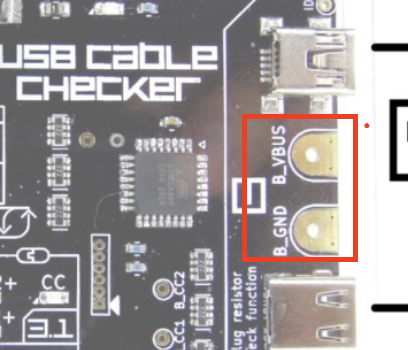
Here are some general tips you can follow while designing an edge connector:
Personally, I would make the edge connector myself, as it would vary from PCB to PCB depending on the functionality.
Awesome thanks! For now I just have the footprint with a User Drawing line to represent the edge cut, which I draw on the pcb schematic. It’s easier to edit than going back into the footprint like you said.
Thanks for the tip on ENIG finish, I think I’ll try it out.