KiCAD is such an incredible software which is completely free! But those who are just getting started might get overwhelmed by the amount of options and settings it has to offer. So learning each tool without real world examples would be hassle.
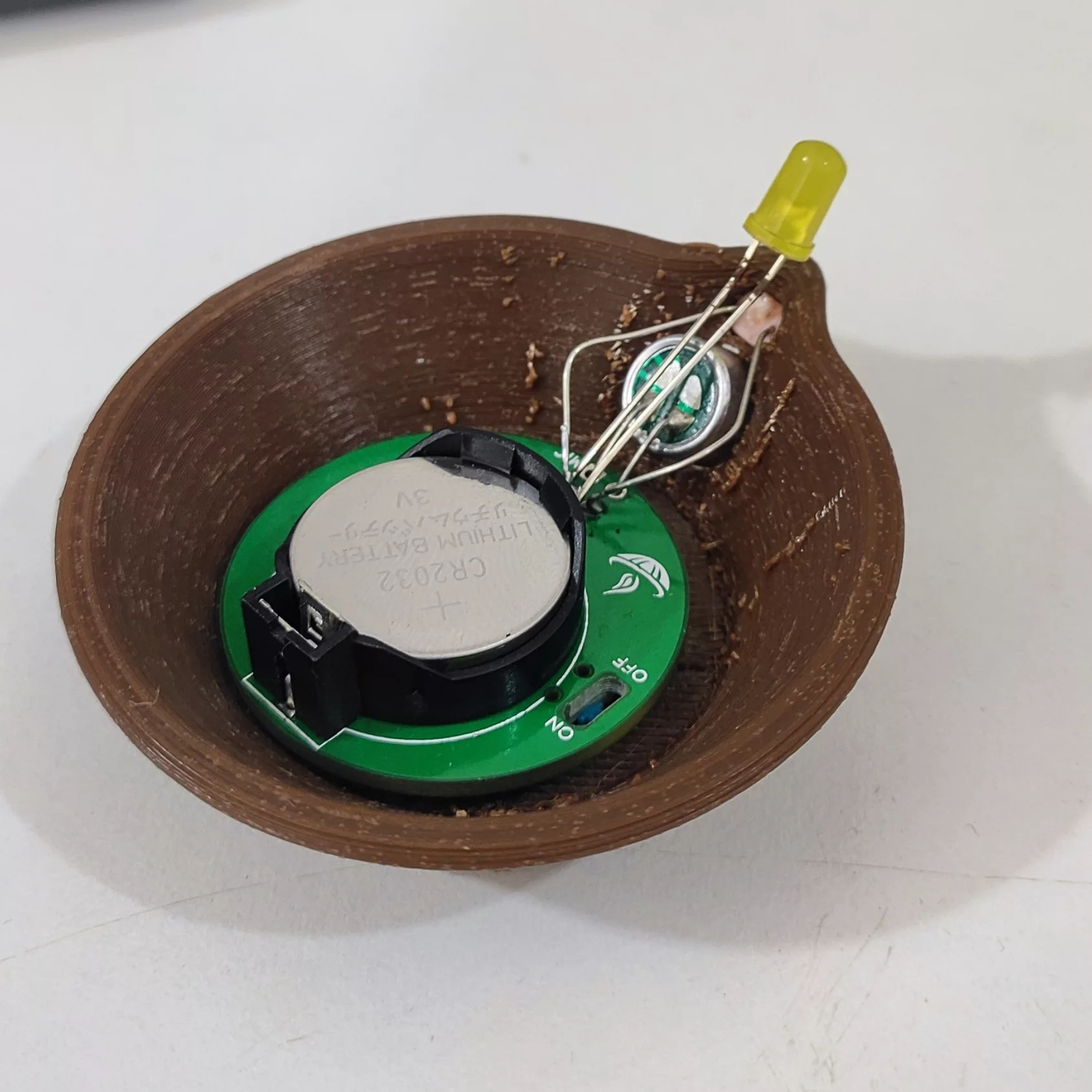
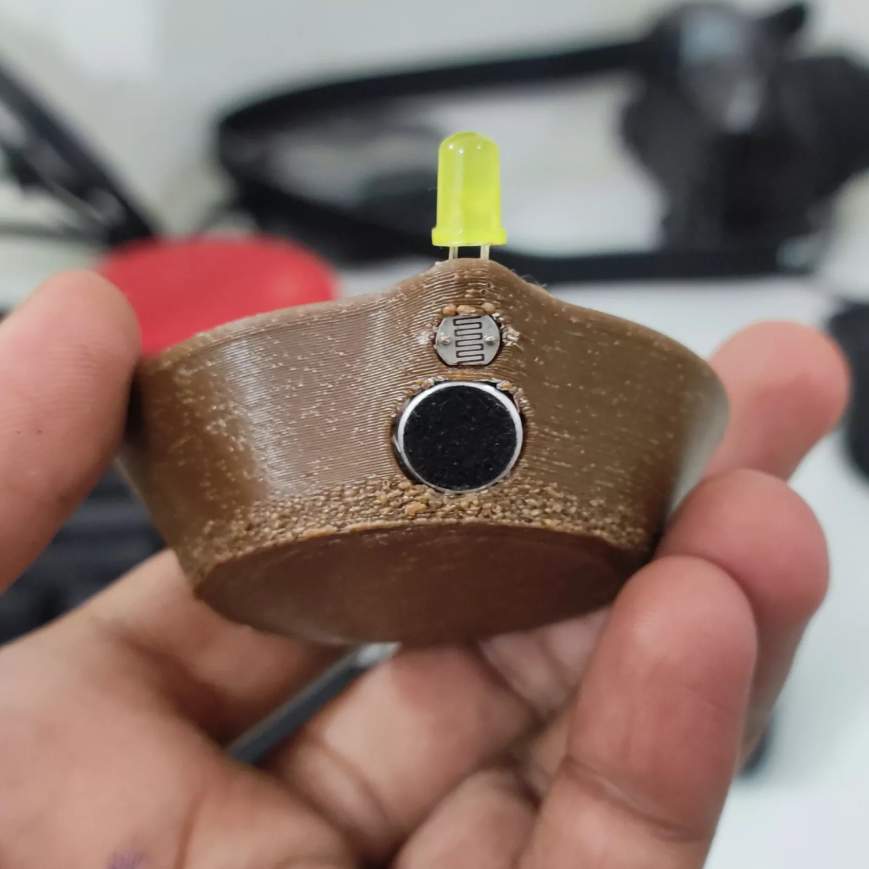
So, in this follow up article of our ‘KiCAD (7.0) tutorial‘ series, we’ll select an interesting project and build a circuit diagram using a schematic editor in KiCAD. The project that we are going to work with is a digital diya, which responds to light, sound and act almost like a real diya! (If you want to learn more about this project, click here)
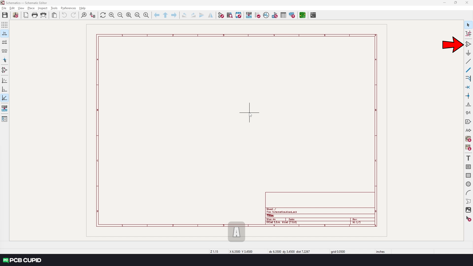
To start, we’ve to create a new project and open the schematic file. From our previous article you should be familiar with the basic editor tools and how to navigate around KiCAD schematic editor.
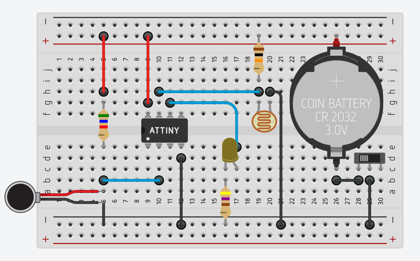
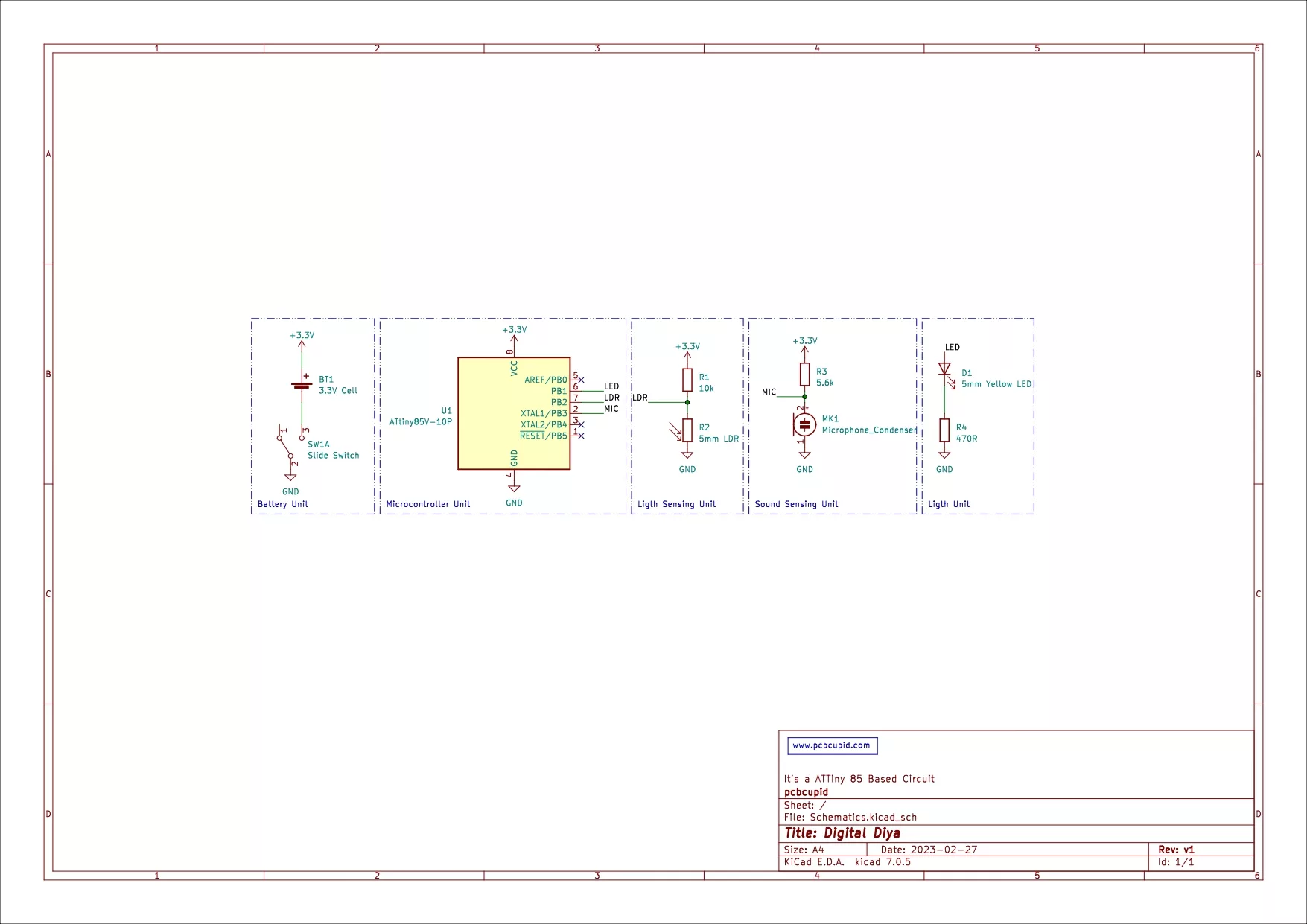
In this article, we’ll focus on few tools on right side tool bar and try to convert the circuit shown below into KiCAD schematics.
Choosing The Component
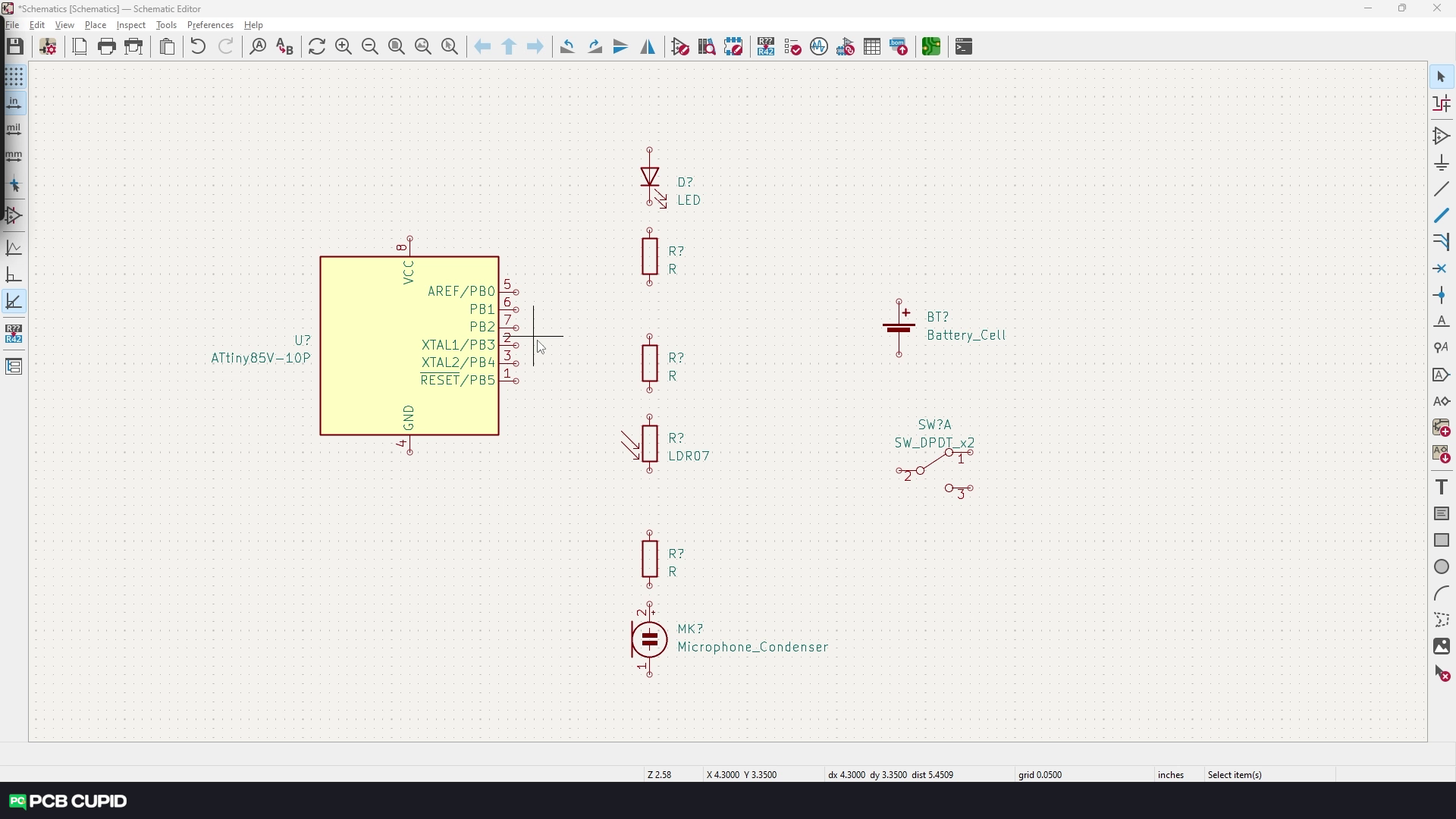
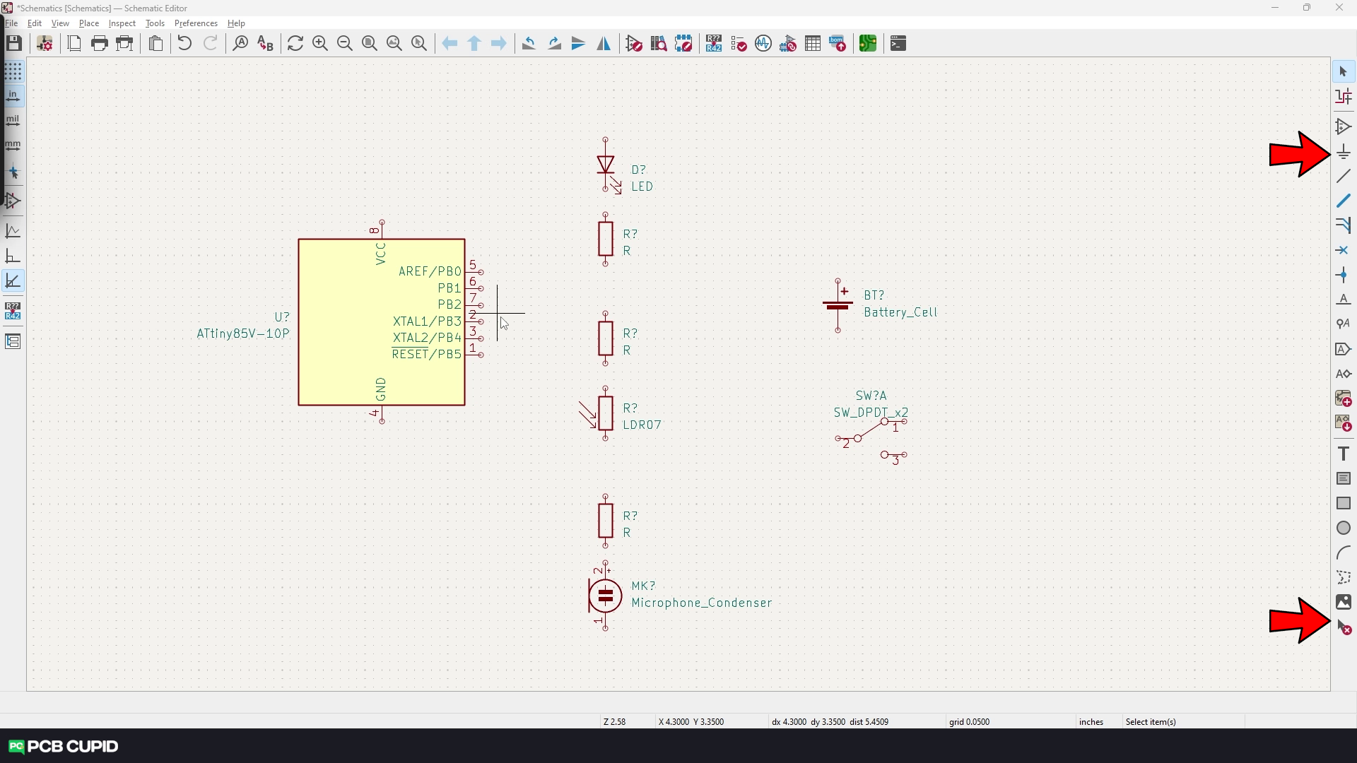
To begin, we need components like an ATtiny85 microcontroller, a few resistors and a few other components. Let’s start by placing those components on the drawing sheet.
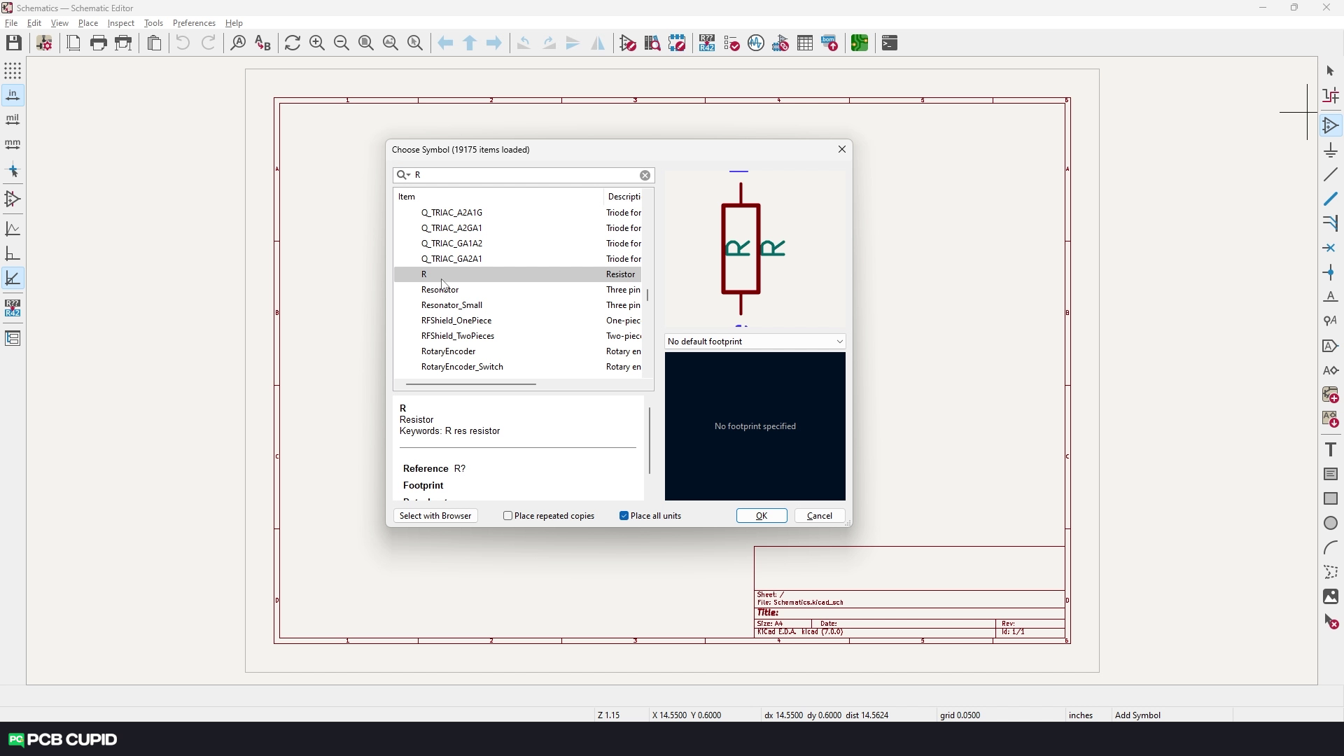
To get those components we can either use the shortcut ‘A’ or you can click on the ‘Add a symbol‘ button as shown in the figure. This will bring up the component search menu. We can search and add the components that we need from this pop up.
Personally we love the way they have arranged all the components and how we can search for it. For example, when we need a resistor, just typing ‘R’ and for capacitor just typing ‘C’ would fetch the respective component! This is true for many basic components.
Component Placement
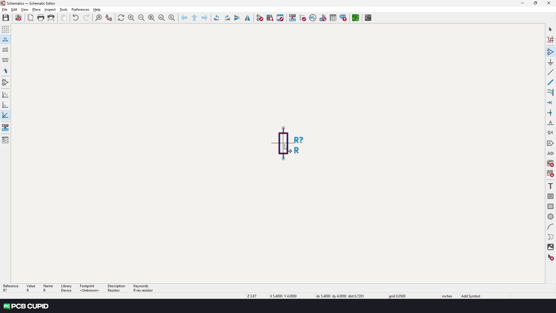
For this particular circuit, let’s start with resistors, so just type ‘R‘ and click on ‘OK‘. Now the component symbol will just follow the cursor and once you do a left click the component is placed on the document.
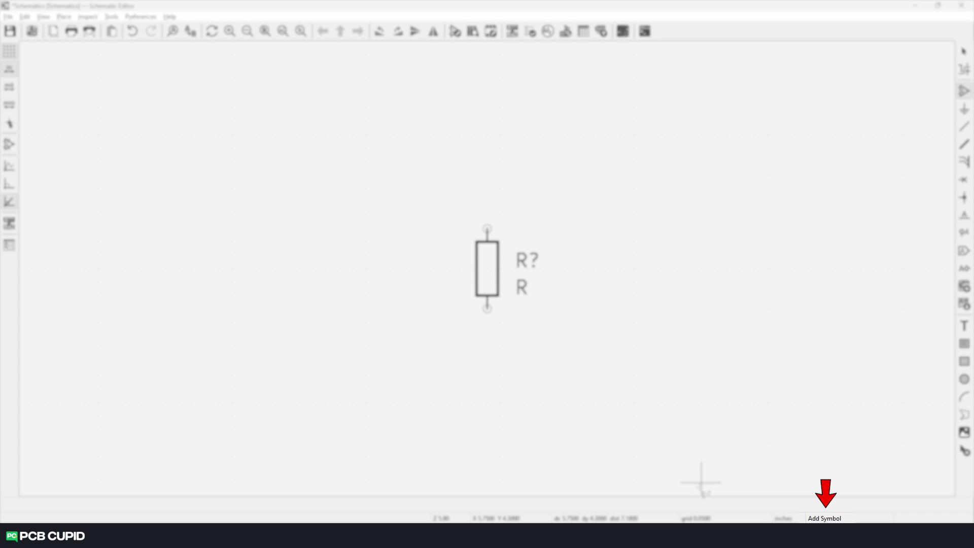
Quick note: You can always look at the bottom status bar to know which tool you have currently selected and you can use the escape key to go back to the default selection tool.
To place anther component, just click on the schematic editor to add another component. Let’s place the resistor in a different orientation this time. For this you can use the key ‘R’ to rotate the component. This will rotate the symbol but it won’t place it on the schematic editor until we do a left click.
To move the resistors, hover the cursor over the symbol and press ‘M’, now we can move around the resistor and change the orientation of the symbol when we press ‘R‘ key. To place the component, just do a left click.
The ATtiny85 pinout look might look a bit odd and might not seem like standard conventional numbering of left to right. This is just to optimize the symbol on the circuit diagram and make it look neat. Usually the positive power symbol (VCC) is placed on the top and the Ground (GND) is placed on the bottom. And in some cases a few pins would be grouped together for easier understanding.
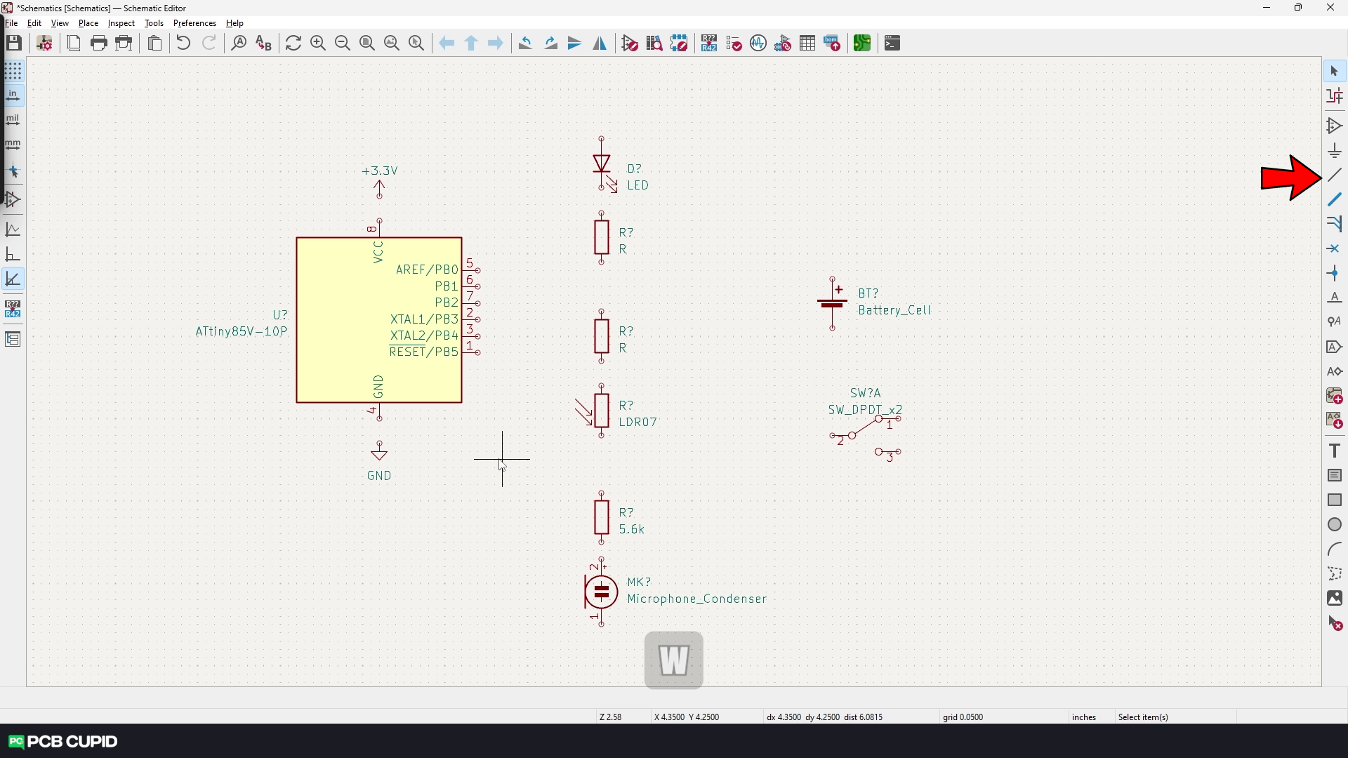
We haven’t placed the symbols for the power and ground yet. That’s because we can access this in multiple ways. We can either use the add symbol button and search for the ground and power like we did before or we can use the next button on the list “add power symbol” to search specifically only power symbols.
To delete any component from the schematic editor, we can easily delete by using the ‘Delete clicked items‘ tool on the bottom right corner and click on the component that should be deleted or we can just hover over the symbol and hit the delete key on the keyboard.
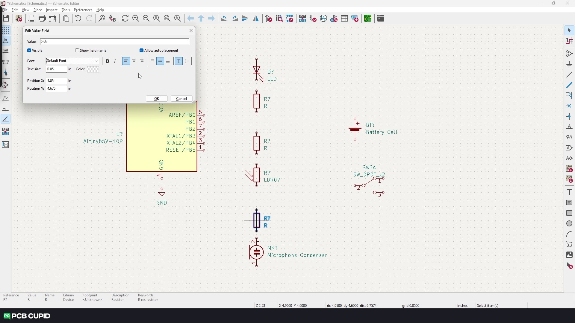
Edit Component Values
Notice something missing? Yes! The values of the symbols. Currently they are just set with their default value. We can change this by hovering over the symbol and pressing ‘V‘. In the pop-up window, we can change the value of the symbol and customize the way they look, but let’s keep them to their default for now.
The additional mnemonics are called designators, they are currently mentioned with ‘?’ because we have turned off the automatic annotation. Once we complete the circuit let’s see how to automatically number them.
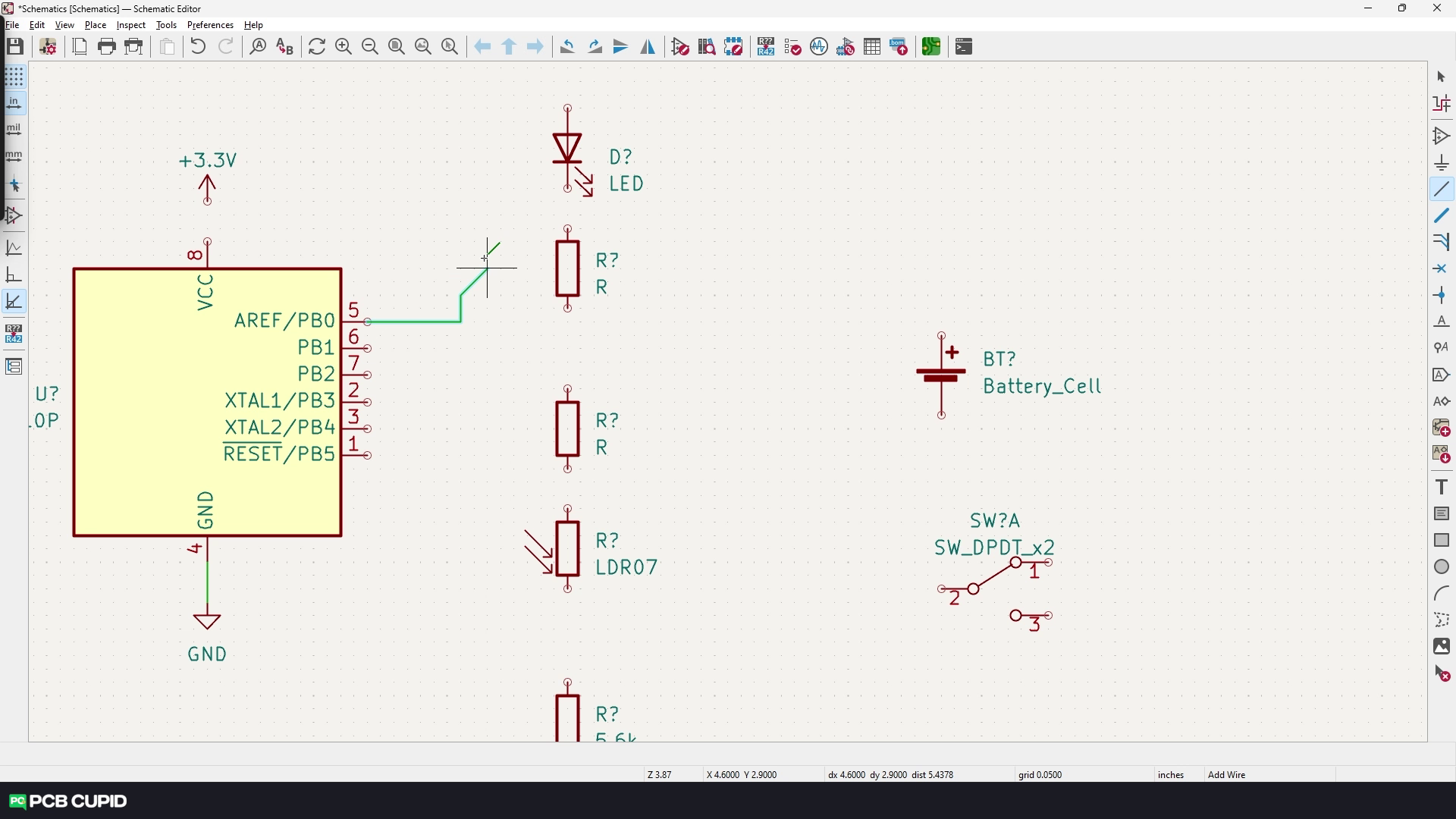
Connecting the Components
Now we have all the components on the schematic editor and if we like their placement we can start connecting them together with wires.
Click on the button below the power symbol or press the key ‘W’ to activate the wiring mode.
We can make the wire connections by just clicking on one pin and then clicking on the pin of the other symbol. To control the way the wire is connected we can use left click while moving to the next component.
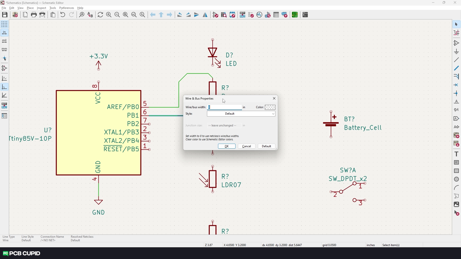
To change the appearance of these wires that connect the symbols, just hover over them and press ‘E‘. But we prefer to keep them as default.
Now, continue the process until the circuit is completed.
Here, we barely used a few tools to do a complete circuit diagram for a project. This is good enough if one wants to just share the circuit diagram with anyone but this is not sufficient to build a PCB or say to make a complicated circuit. But so far, this is very good progress!
In the next article, we’ll learn how to use the rest of the tools on the right tool bar and make sure that the circuit looks better. Until then, if you have any questions, you can ask in our forum here. Keep learning and Keep creating!


Leave a comment