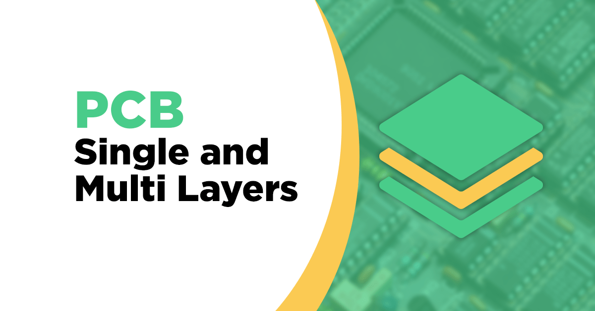
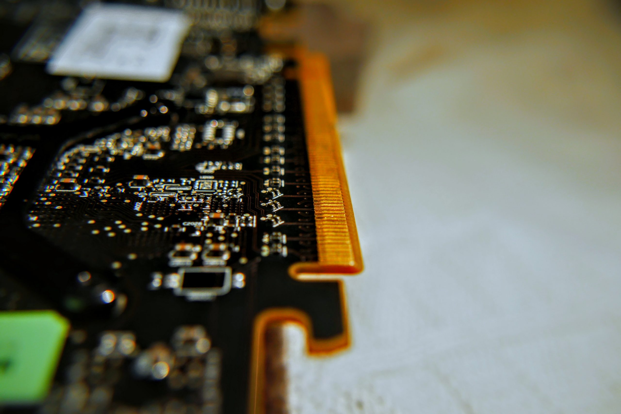
Printed Circuit Boards made the break-through because of their miniature size and compact design platforming all the required electronic components.
However, depending on the applicability the PCB can be made into multi-layered stacked one on top of another. This makes space for placing more components. Since both single and multi-layered PCBs are manufactured and widely used it is important that one should be aware of differences between them, their usability and designing.
How are Single and Multi-Layered PCBs Different?
In Terms of Design:
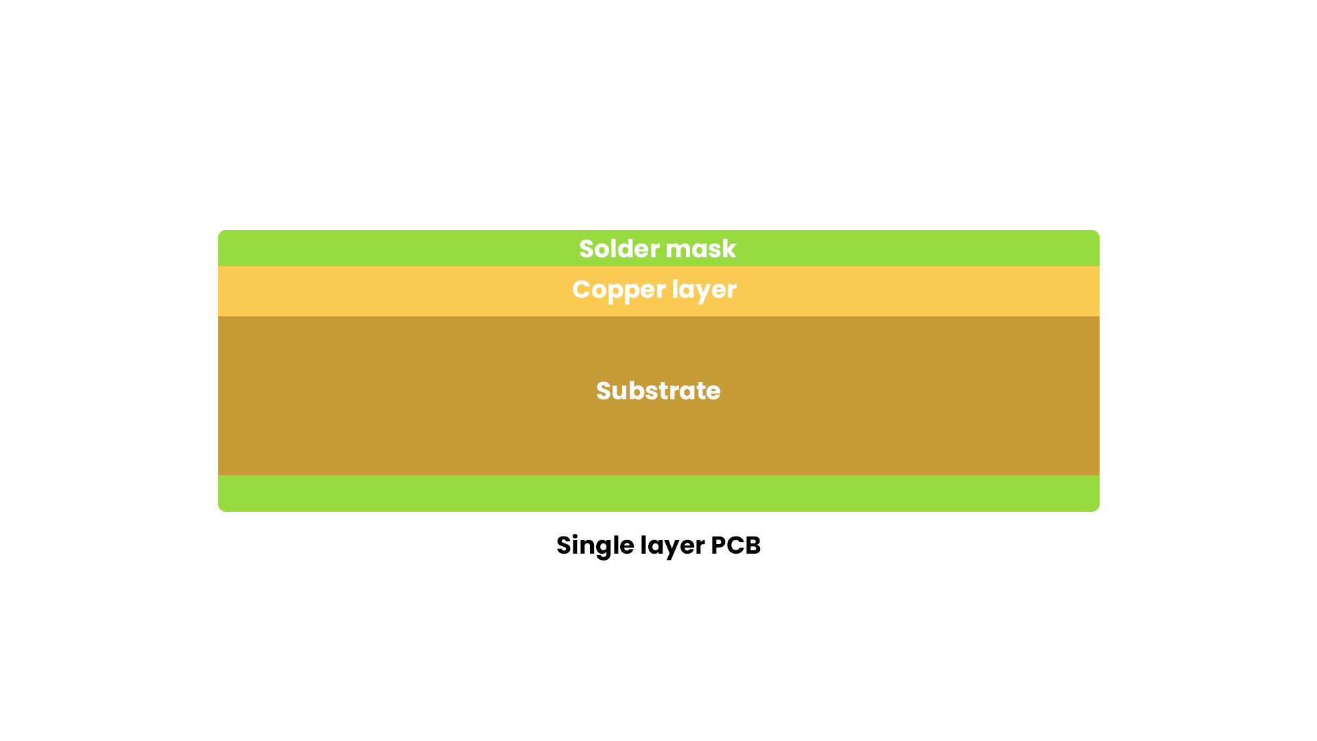
Single layered PCBs have substrate material on top of which the top layer is placed. This top layer is the conductive copper layer. The protective layer of the solder mask is applied on both sides of the substrate while the top layer will be only on one side. On this top layer the components will be assembled.
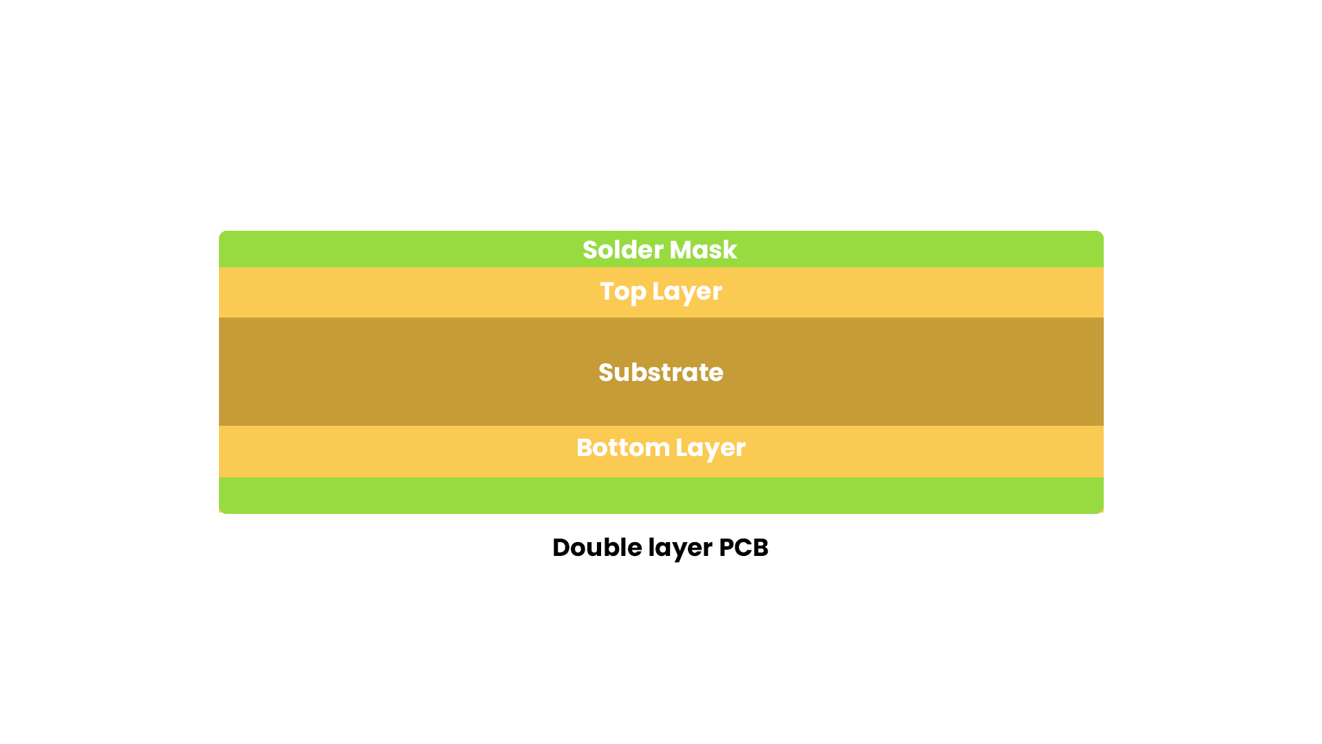
Multi-layered PCBs can be double layered or more than that. In case of double layered or 2-layered, there is only one substrate like the single layer but the conductive layer will be attached to both the top and bottom layer of the substrate.
Multi-layered PCBs above 2-layered, the layers are mostly in even numbers like 4-layered or 6-layered and so on. Multi-layered PCBs have more than one substrate, attached to each other with the help of adhesive and these layers are also insulated from each other to avoid mishap. The protective solder mask and the silk screen is applied only to the top most and the bottom most layers of the stack.
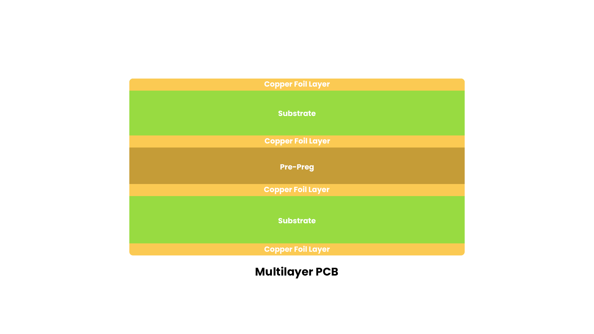
Why do multi-layered PCBs are mostly in even numbers?
This is to avoid problems of wrapping and twisting of PCB post soldering. The even layers provide strength that balances out while in case of odd numbers there can be imbalance.
In Terms of Manufacturing Process:
Single layer: the components are placed on the conductive layer (the top layer) while the conductor pattern is on the other side (the bottom layer).
Double layer: Both the components and the circuits are connected on either side of the substrate on top of the conductive layer. These are connected with each other through pathways called vias.
In Terms of Suitability:
Single Layered PCB:
- Suitable for basic circuit designs and simple functioning.
- For storing only a small amount of data.
- Mainly to develop low circuit designs.
- These are mostly used in small household appliances like coffee machines and technology devices like calculators, printers, etc.
Multi-Layered PCB:
- Suitable for devices for more complex functioning and require complex capabilities.
- For storing higher data, thus used in devices like mobile phones, laptops, etc.
- Good for developing complex circuit designs.
- Suitable for higher signal reliability, thus used in GPS devices, medical and aerospace devices.
Both Have Brighter Sides:

Advantages of Single Layered PCB:
- Lower production cost and lead time.
- Manufacturing process is easy and thus easy to design for an amateur.
- Due to higher manufacturing speed, a large volume of PCBs can be produced.
- Chances of overlaps and intersections are very low.
- Easy to troubleshoot, debug and repair.
Advantages of Multi-Layered PCB:
- Higher reliability and functionality.
- More flexible in circuit routing.
- Smaller size and lightweight.
- Meets the space constraint in circuit design thus are very favourable in advanced technology.
Both Have Darker Sides:

Disadvantages of Single Layered PCB:
- Not suitable for advanced technology and demanding applications.
- They have lower speed, larger size and higher weight, thus occupying more space.
- Less flexibility in circuit routing.
Disadvantages of Multi-Layered PCB:
- Due to stacking of layers and complex production process lead time is more.
- Manufacturing cost is higher than single layered PCBs.
- Since manufacturing speed is slow, large volumes of PCBs cannot be produced.
- Difficult to troubleshoot and repair.
- There is an intersection and overlap of traces.
How to Choose Between Single and Multi-Layered PCBs:

Based on following criteria the selection should be done:
- Functional needs of the device: For simpler needs single layered is apt while for complex functioning multi-layered is suited.
- Size Constraints: To make the device more compact, a multi layered PCB is more suitable. In laptops upto 12-14 layered PCBs are used.
- Manufacturing Budget: Single layered PCB will cost less.
- Reliability and Durability: Multi-layered PCBs are more reliable and durable when in comparison to single layered.
- Lead Time: When there is time crunch, single layered PCBs are ideal.
As a beginner it is important to be aware of nuances related to PCB layering. Being aware of pros and cons of single and multi-layered PCB is important before making decisions related to PCB manufacturing. While both have their plus and minus, as a starter, one should begin with a single layered PCB first, learn about its assembly and then move to multi-layered that involves more design rules and complex manufacturing process.
You can follow us on Instagram for quick tips and tricks like this.


Leave a comment